
High optical efficiency CMOS image sensor

a high optical efficiency, image sensor technology, applied in the direction of basic electric elements, electrical equipment, semiconductor devices, etc., can solve the problem of achieve high optical inter-pixel optical isolation, and high fill factor

Active Publication Date: 2012-07-26
HONG KONG APPLIED SCI & TECH RES INST
View PDF2 Cites 11 Cited by
  • Summary
  • Abstract
  • Description
  • Claims
  • Application Information

AI Technical Summary

Benefits of technology

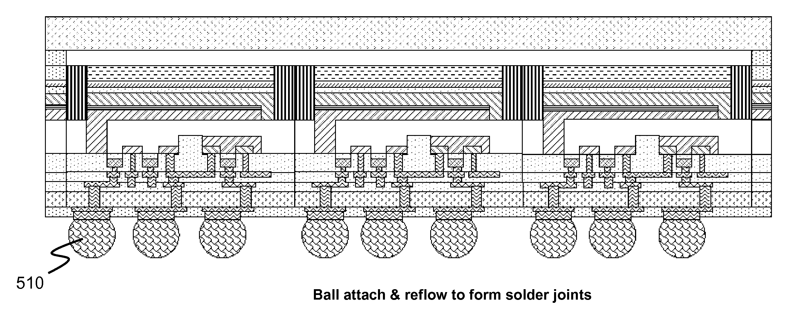
[0007]The present invention provides high optical efficiency CMOS image sensors capable of sustaining pixel sizes less than 1.2 microns. The sensors include isolation grids that border each pixel and block incident light penetration into adjacent pixels. This results in high optical inter-pixel optical isolation. The image sensor photodiodes possess high fill factors. This feature, coupled with the isolation grids, permit image sensors without microlenses to be fabricated, optionally having pixel sizes less than 1.2 microns, resulting in increased sensor pixel density. Consequently, high resolution image sensors can be formed.
[0008]The present invention provides a high optical efficiency CMOS image sensor that includes plural imaging pixels, each pixel including a photodiode structure on a semiconductor substrate, the photodiode structure being positioned adjacent a light-incident upper surface of the image sensor. An isolation grid surrounds each photodiode structure and defines the pixel boundary. The isolation grid extends to a depth of at least the thickness of the photodiode structure and is configured to prevent light incident on the pixel from penetrating through the incident pixel to an adjacent pixel. Optionally, the isolation grid extends substantially through the depth of the semiconductor substrate, preventing electrical crosstalk between adjacent pixels.

Problems solved by technology

This results in high optical inter-pixel optical isolation.

Method used


Image

  • High optical efficiency CMOS image sensor
  • High optical efficiency CMOS image sensor
  • High optical efficiency CMOS image sensor

Examples


Embodiment Construction

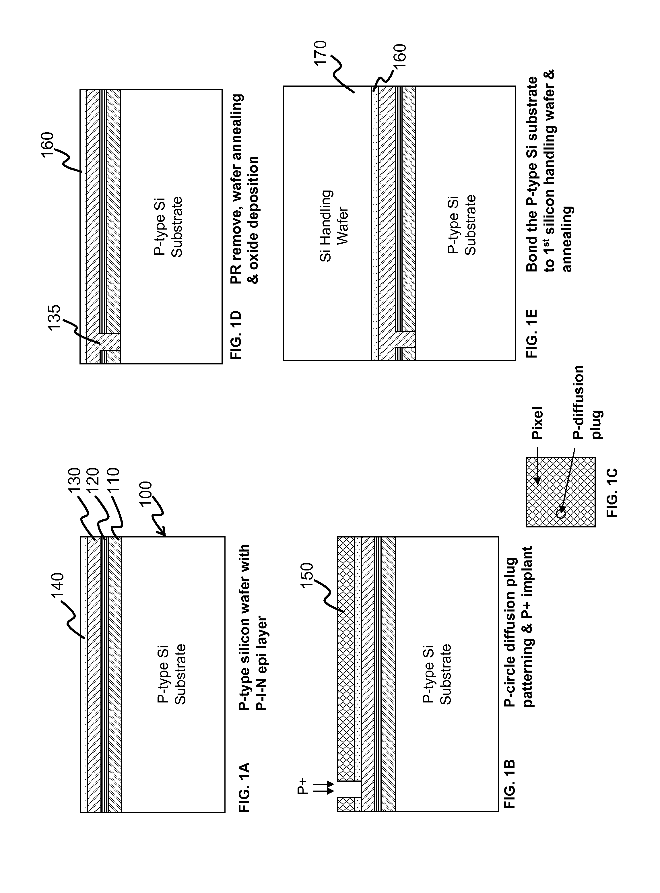
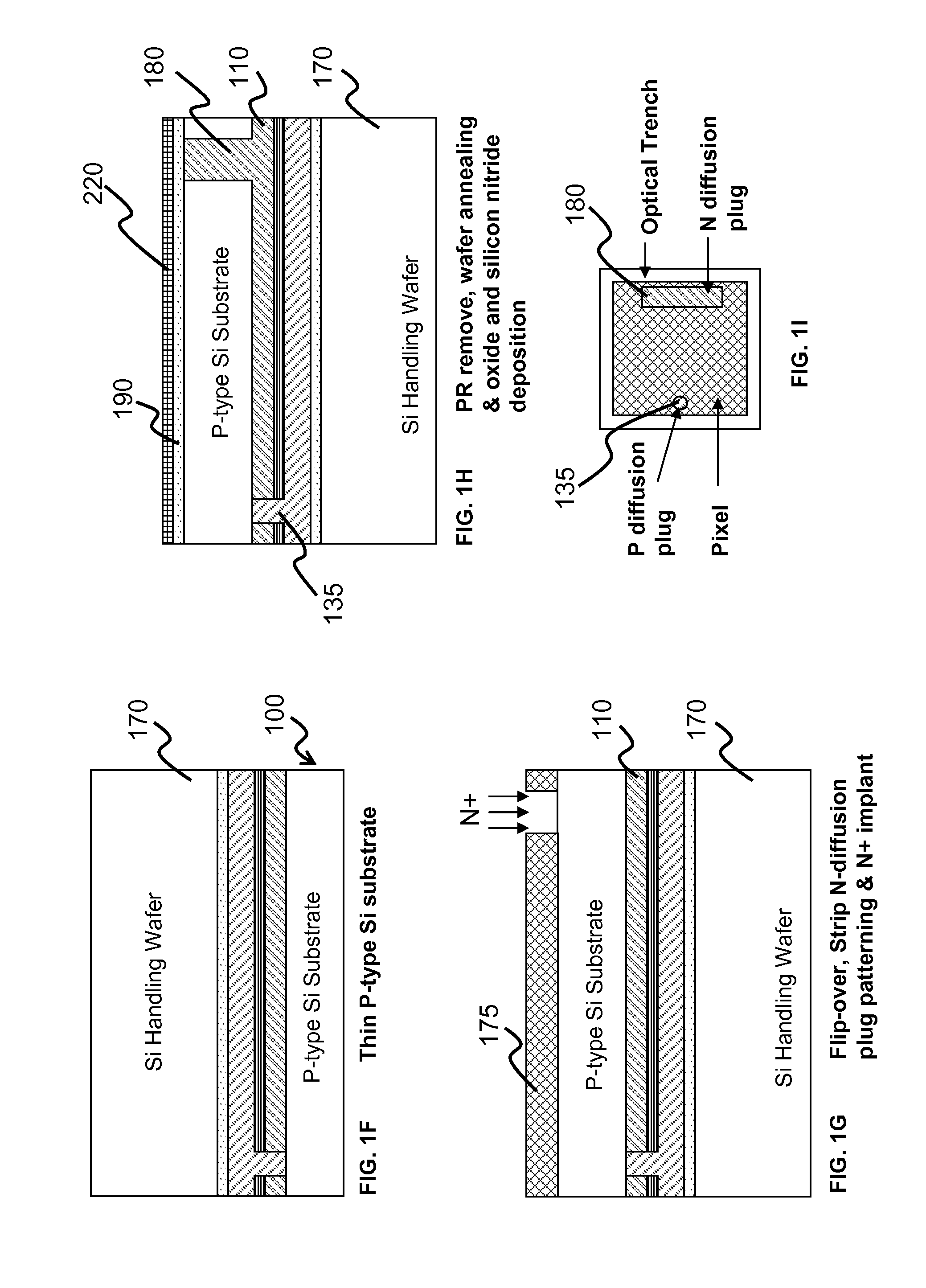
[0013]The fabrication of a CMOS image sensor having isolation grids is depicted with respect to the drawings in which FIG. 1A depicts a cross-sectional view of a p-doped silicon wafer 100 having a photodiode structure formed thereon. In this exemplary embodiment, the photodiode structure is an epitaxial p-i-n layer structure formed on the substrate; however, any photodiode structure can be used in the image sensor of the present invention. The n-layer (n-doped silicon) is designated as 110, the i-layer (intrinsic or non-doped silicon) as 120 and the p-layer (p-doped silicon) as 130. It is noted that all of the processes of the present invention rely on well-established CMOS fabrication techniques; therefore, detailed description of the process conditions is well-known to those of ordinary skill in the art. Any CMOS processing technique can be used to form the various layers and structures of the present invention.

[0014]A glass / SiO2 layer 140 is formed over the p-i-n structure. A pat...


PUM


Abstract

High optical efficiency CMOS image sensors capable of sustaining pixel sizes less than 1.2 microns are provided. Due to high photodiode fill factors and efficient optical isolation, microlenses are unnecessary. Each sensor includes plural imaging pixels having a photodiode structure on a semiconductor substrate adjacent a light-incident upper surface of the image sensor. An optical isolation grid surrounds each photodiode structure and defines the pixel boundary. The optical isolation grid extends to a depth of at least the thickness of the photodiode structure and prevents incident light from penetrating through the incident pixel to an adjacent pixel. A positive diffusion plug vertically extends through a portion of the photodiode structure. A negative diffusion plug vertically extends into the semiconductor substrate for transferring charge generated in the photodiode to a charge collecting region within the semiconductor substrate. Pixel circuitry positioned beneath the photodiode controls charge transfer to image readout circuitry.

Description

FIELD OF THE INVENTION[0001]The present invention relates to CMOS image sensors in general and, more particularly, to CMOS image sensors having high optical efficiencies, high fill factors, and low optical and electrical crosstalk.BACKGROUND OF THE INVENTION[0002]Solid state imaging devices such as charge coupled devices (CCDs) and complementary metal oxide semiconductor (CMOS) image sensors are widely used in imaging applications ranging from cameras to mobile telephones and computers. Because CMOS manufacturing technology is compatible with the formation of other semiconductor devices, it is possible to integrate CMOS image sensors with other devices.[0003]CMOS image sensors fall broadly into two categories: front side illumination sensors and back side illumination sensors. In front side illumination devices, the photodiode that captures the photons is positioned relatively far from the incident light. Thus back side illumination devices, in which the photodiode is positioned nea...

Claims


Application Information

Patent Timeline
Patent Type & Authority Applications(United States)
IPC IPC(8): H01L31/113
CPCH01L27/1461H01L27/14618H01L27/1463H01L27/14632H01L27/14692H01L27/1464H01L27/14645H01L27/14687H01L27/1469H01L27/14636H01L24/19H01L2924/12043H01L2924/00
Inventor LAW, PUI CHUNG SIMONYANG, DANSHI, XUNQING
Owner HONG KONG APPLIED SCI & TECH RES INST
Learn More