Impedance-Matching Network Using BJT Switches in Variable-Reactance Circuits

a variable-reactance circuit and network technology, applied in the field ofplasma processing, can solve the problems of only having two terminals, resistive elements in the network, high cost of pin diodes, and high cost, and achieve the effect of lowering the voltag

Active Publication Date: 2012-07-26
AES GLOBAL HLDG PTE LTD
View PDF0 Cites 72 Cited by
  • Summary
  • Abstract
  • Description
  • Claims
  • Application Information

AI Technical Summary

Benefits of technology

[0010]Even though the BJT can handle high voltage, its voltage-handling threshold may not be as great as that of a vacuum variable capacitor. As a result, the classic topologies suitable for using vacuum variable capacitors may be adapted to lower the voltage that the BJT experiences in the match network during normal operation.

Problems solved by technology

The only resistive elements in a match network are typically associated with losses in non-ideal reactive and lossless components or components that do not take part in the impedance transformation such as components for sensing voltage, current, power or temperature.
However, PIN diodes are very expensive and only have two terminals.
Thus, the RF current and the DC control current must enter via the same terminal requiring complicated, expensive, and bulky circuitry (e.g., inductors) to isolate the DC control source from the RF source.
Even though the BJT can handle high voltage, its voltage-handling threshold may not be as great as that of a vacuum variable capacitor.

Method used


Image

  • Impedance-Matching Network Using BJT Switches in Variable-Reactance Circuits
  • Impedance-Matching Network Using BJT Switches in Variable-Reactance Circuits
  • Impedance-Matching Network Using BJT Switches in Variable-Reactance Circuits

Examples


Embodiment Construction

[0038]This disclosure will begin with a discussion of the problems faced, unexpected results discovered, and proposed device physics to explain the unexpected results.

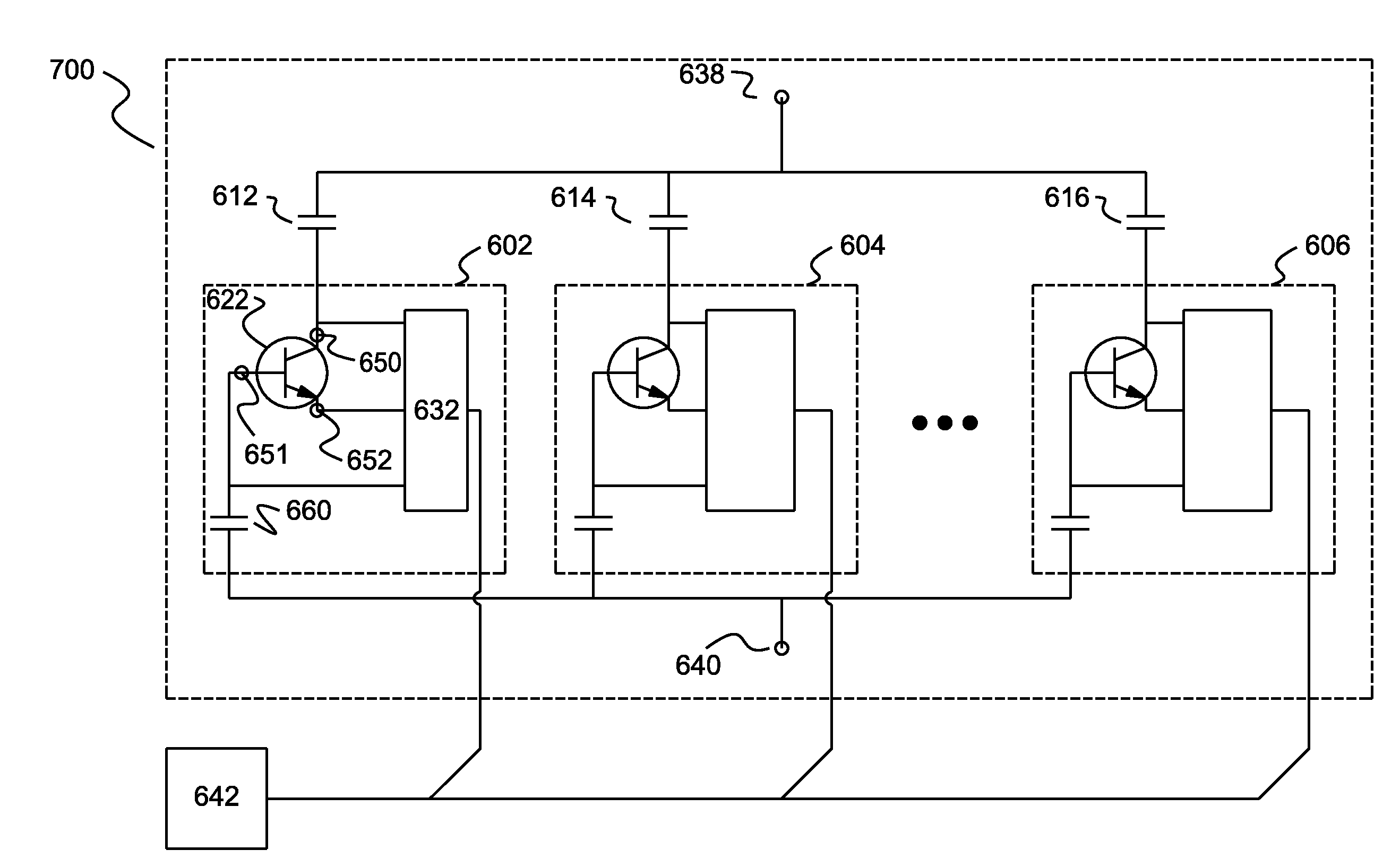
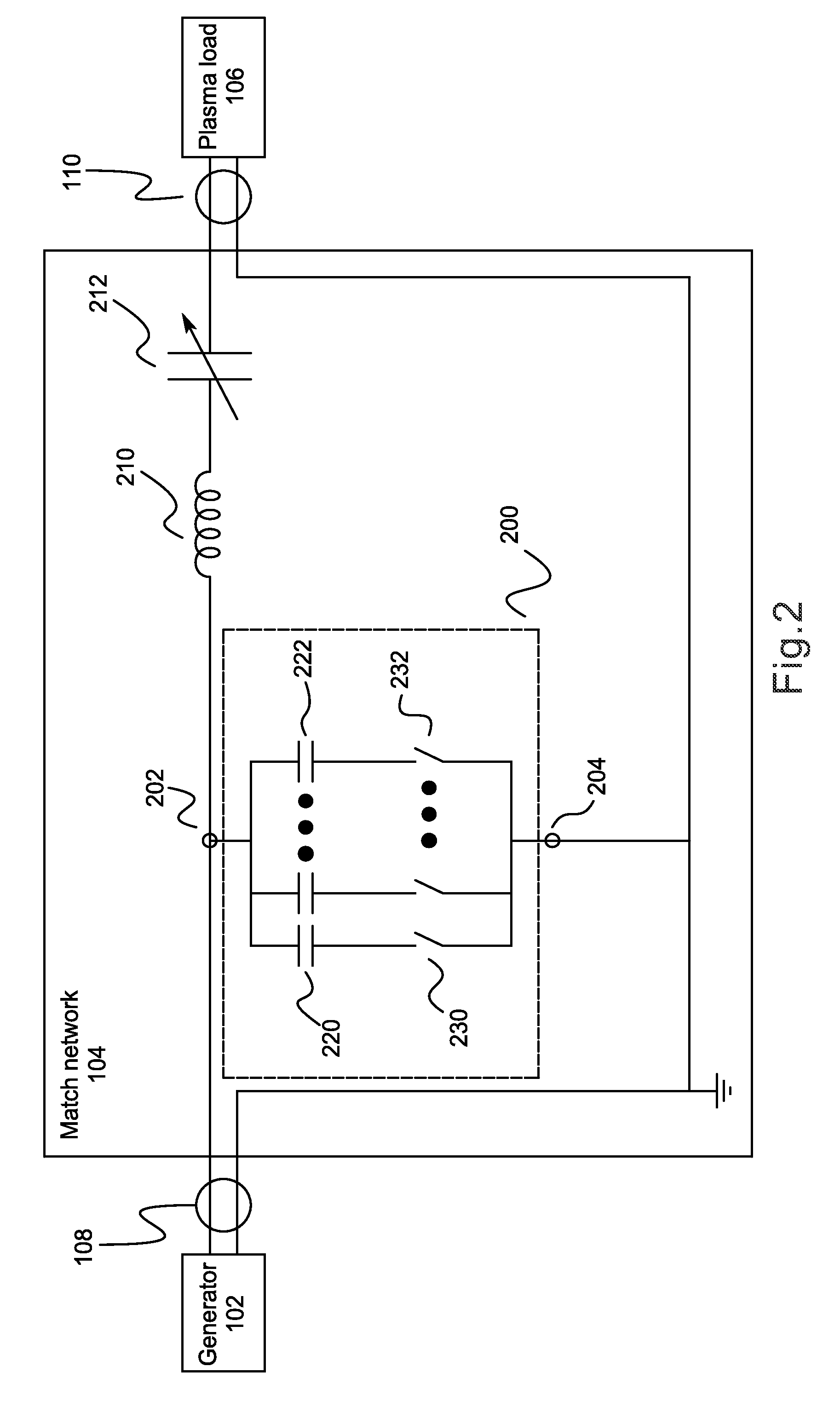
[0039]A device is needed that can fulfill the role of a PIN diode as a switch for shorting capacitors or other reactive circuits between two terminals in order to create a variable reactance element for use in an impedance-matching network. This device should have low losses in both the on and off-states. It should also handle high voltage in the off-state and high current in the on-state. Switching control should be enabled via a terminal other than a terminal that passes RF current, thereby avoiding complicated, bulky, and expensive isolation circuitry. Unexpectedly these goals are achieved via a previously undiscovered bipolar junction transistor (BIT) mode of operation as described herein.

[0040]Typically, a BJT operated as a switch, conducts current between collector and emitter in an on-state, and blocks the flow ...


PUM


Abstract

This disclosure describes systems, methods, and apparatuses for impedance-matching radio frequency power transmitted from a radio frequency generator to a plasma load in a semiconductor processing chamber. Impedance-matching can be performed via a match network having a variable-reactance circuit. The variable-reactance circuit can comprise one or more reactive elements all connected to a first terminal and selectively shorted to a second terminal via a switch. The switch can comprise a bipolar junction transistor (BJT) or insulated gate bipolar transistor (IGBT) controlled via bias circuitry. In an on-state, the BJT base-emitter junction is forward biased, and AC is conducted between a collector terminal and a base terminal. Thus, AC passes through the BJT primarily from collector to base rather than from collector to emitter. Furthermore, the classic match network topology used with vacuum variable capacitors can be modified such that voltages do not overload the BJT's in the modified topology.

Description

FIELD OF THE INVENTION[0001]The present invention relates generally to plasma processing. In particular, but not by way of limitation, the present invention relates to systems, methods and apparatuses for impedance-matching radio frequency power transmitted from a radio frequency generator to a plasma load in a semiconductor processing chamber.BACKGROUND OF THE INVENTION[0002]In the semiconductor manufacturing world, manufacturers produce plasma processing chambers that utilize radio frequency (RF) power to generate a plasma. In order to achieve efficient power transfer between the RF generator (“generator”) and the plasma load, an impedance-matching network (“match network”) is often used to match the load impedance to a desired input impedance, typically 50 ohm. Plasma load impedance may vary depending on variables such as generator frequency, power, chamber pressure, gas composition, and plasma ignition. The match network accounts for these variations in load impedance by varying...

Claims


Application Information

Patent Timeline
Patent Type & Authority Applications(United States)
IPC IPC(8): H03H11/00H03K3/00
CPCH01J37/32183H03H5/12H03H7/38H03K17/16H05H1/46H05H2001/4682H03H11/30H03K17/68H03K17/60H05H2242/26
Inventor VAN ZYL, GIDEON J.GUROV, GENNADY G.
Owner AES GLOBAL HLDG PTE LTD
Why Eureka
Try Eureka