
Method for achieving four-bit storage using flash memory having splitting trench gate

a trench gate and flash memory technology, applied in the field of nonvolatile semiconductor memory, can solve the problems of flash memory having such structure with serious reliability problems, flash memory with such structure may be faced with serious crosstalk problems, etc., and achieve the effects of improving device performance, increasing storage density, and high density

Inactive Publication Date: 2012-07-26
PEKING UNIV
View PDF18 Cites 0 Cited by
  • Summary
  • Abstract
  • Description
  • Claims
  • Application Information

AI Technical Summary

Benefits of technology

[0008]An object of the present invention is aimed to meet a huge requirement for a nonvolatile semiconductor memory of a high density in a current electronics market. In the invention, a function of a four-bit storage is achieved by changing a programming mode based on a device structure proposed in a Chinese patent 200710105964.2, so that a performance of the device is improved while a storage density is increased.

Problems solved by technology

If there is a leakage path existed in a tunneling oxide layer, all electrons stored in the floating gate may be leaked out through the path.
Therefore, in a case that the oxide layer is usually thin in a small size memory, the flash memory having such structure may be faced with a serious problem in terms of reliability.
Since the charges stored at both ends of the channel are close to each other, a very serious problem of crosstalk is existed.

Method used


Image

  • Method for achieving four-bit storage using flash memory having splitting trench gate
  • Method for achieving four-bit storage using flash memory having splitting trench gate

Examples


Embodiment Construction

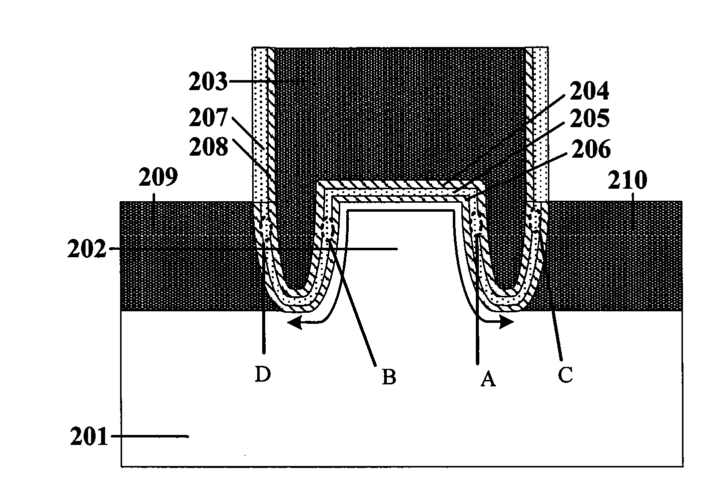
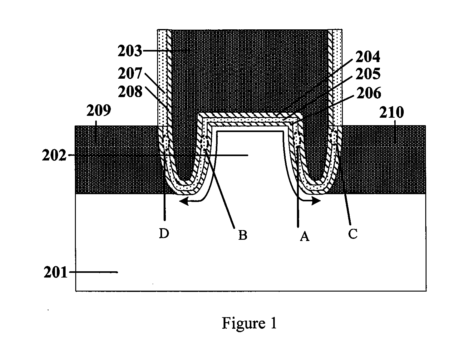
[0028]Hereinafter, a disclosure of the present invention is further described in more detail through embodiments.

[0029]A practical operation of the present invention is illustrated with respect to two cases, in which one case is storage bits of a silicon nitride trap layer at an inner side of a trenches, and the other is storage bits of a silicon nitride trap layer at an outer side of a trench.

[0030]1. Storage bits of the silicon nitride trap layer at the inner side of the trench

[0031]Programming:

[0032]A device as shown in FIG. 1 has a symmetric structure. Thus, either of the n+ region 209 or 210, which are disposed at both ends of the device, may be used as a source or a drain. When a region A is to be programmed, the region 210 is used as the drain, and the region 209 is used as the source. When programming, a positive voltage Vd (about 4V) is applied to the drain terminal 210; the source terminal is grounded; a relatively high positive voltage Vg (about 12V) is applied to the con...


PUM


Abstract

The present invention discloses a method for achieving four-bit storage by using a flash memory having a splitting trench gate. The flash memory with the splitting trench gate is disclosed in a Chinese patent No. 200710105964.2. At one side that each of two trenches is contacted with a channel, a programming for electrons is achieved by using a channel hot electron injection method; and at the other side that each of the two trenches is contacted with a source or a drain, a programming for electrons is achieved by using an FN injection method, so that a function of a four-bit storage of the device is achieved by changing a programming mode. Thus, a performance of the device is improved while a storage density is greatly increased.

Description

CROSS-REFERENCE TO RELATED APPLICATION[0001]The present application claims priority to Chinese Patent Application (No. 201010523322.6), filed on Oct. 22, 2010 in the State Intellectual Property Office of People's Republic of China, which is incorporated herein by reference in its entirety.FIELD OF THE INVENTION[0002]The present invention refers to a nonvolatile semiconductor memory in an ultra-large-scale integrated circuit, and particularly relates to a storage method of a multi-bit flash memory having a trench gate structure.BACKGROUND OF THE INVENTION[0003]As one of most rapidly developing fields in a current semiconductor industry, a semiconductor memory is always a research focus in the industry. Particularly, since various consumer electronic products are widely used today, a requirement for a high performance semiconductor memory is ever-increasing. Among them, a flash memory has occupied a very large share in today's memory market due to its advantages such as a compatibilit...

Claims


Application Information

Patent Timeline
Patent Type & Authority Applications(United States)
IPC IPC(8): G11C16/34
CPCG11C16/0475H01L29/7887H01L29/7923H01L29/42352
Inventor CAI, YIMAOHUANG, RUQIN, SHIQIANGTANG, PORENTANG, YUTAN, SHENGHUHUANG, XINPAN, YUE
Owner PEKING UNIV
Learn More