Semiconductor memory device

Active Publication Date: 2012-08-02
SEMICON ENERGY LAB CO LTD
View PDF9 Cites 15 Cited by
  • Summary
  • Abstract
  • Description
  • Claims
  • Application Information

AI Technical Summary

Benefits of technology

[0035]Furthermore, a reduction in capacitance of the capacitor makes it unnecessary to form a structure body with a high aspect ratio, unlike in a conventional DRAM. Accordingly, the bit line can be easily provided over the capacitor.
[0036]Note that in the above structure, since the sub bit line is located below the cell transistor and there is no structure that becomes an obstruction, the depth at which the sub bit line is provided can be arbitrarily determined. Needless to say, the formation of the sub bit line in a position apart from another wiring makes it possible to further reduce the parasitic capacitance. In addition, when the depths of the sub bit lines adjacent to each other are diffe

Problems solved by technology

That is, an extremely long and narrow structure body whose depth or height is 2 μm or more needs to be formed in a limited area, which is difficult to realize with high yield.
When a stacked capacitor is employed, thus many structure bodies are provided over a word line, which results in difficulty in circuit design and manufac

Method used


Image

  • Semiconductor memory device
  • Semiconductor memory device
  • Semiconductor memory device

Examples


embodiment 1

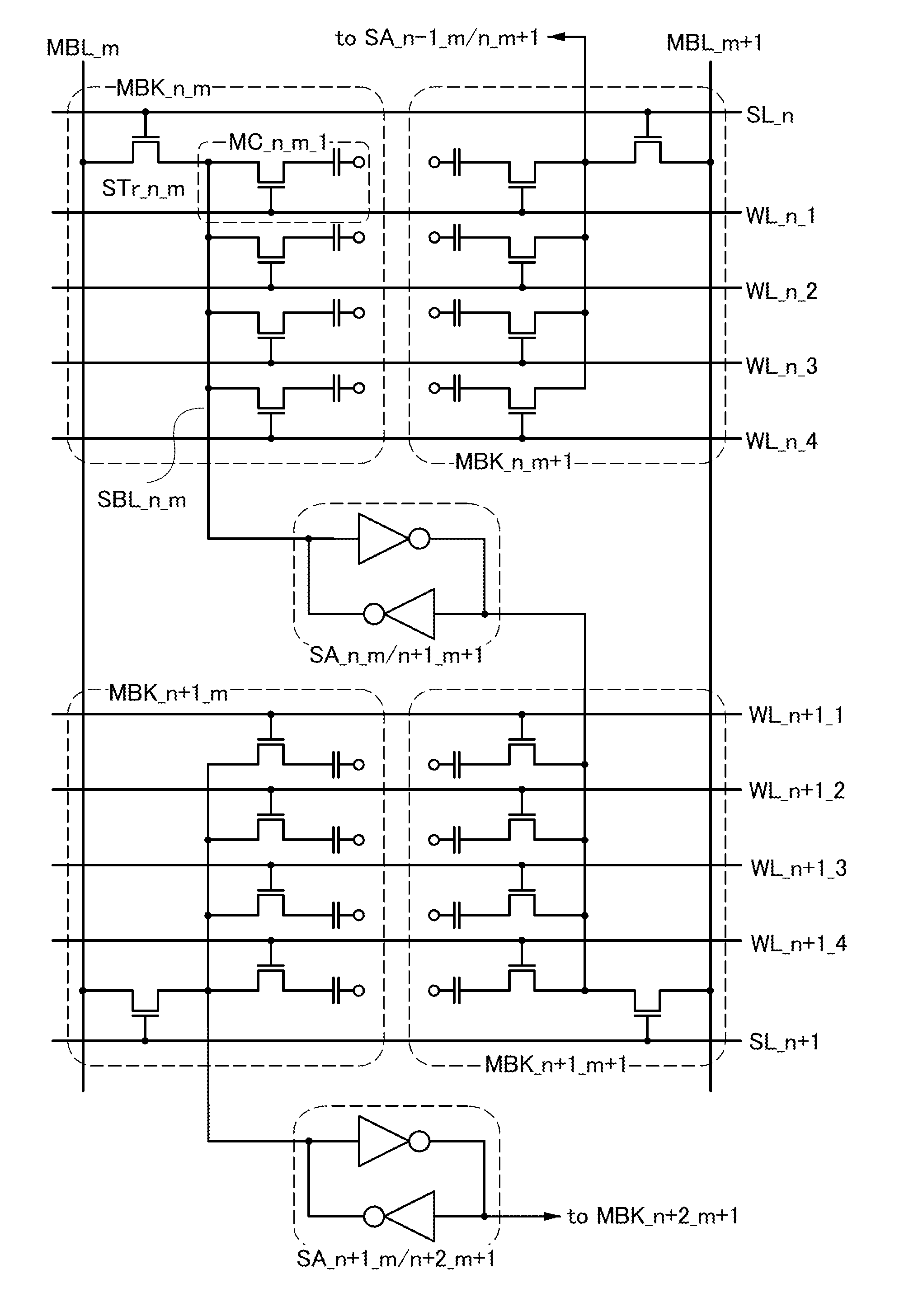
[0049]FIGS. 4A and 4B, FIG. 5, and FIG. 6 illustrate examples of a DRAM circuit to which this embodiment is applied. FIG. 4A illustrates an arrangement of one memory block and a sense amplifier circuit related thereto. As illustrated in FIG. 4A, a memory block MBK_n_m in an n-th row and an m-th column includes a selection transistor STr_n_m, a sub bit line SBL_n_m, and a plurality of (four in FIG. 4A) memory cells MC_n_m_1 to MC_n_m_4.

[0050]Although four memory cells MC are provided in the memory block MBK in FIG. 4A, a larger number of memory cells may be provided. For example, the number of the memory cells MC included in one memory block MBK is preferably 2 to 64. As the number of the memory cells increases, the length of the sub bit line SBL increases, and accordingly parasitic capacitance increases. When the capacitance of the capacitor of the memory cell MC is constant, a ratio of the capacitance of the capacitor of the memory cell MC to parasitic capacitance of the sub bit li...

embodiment 2

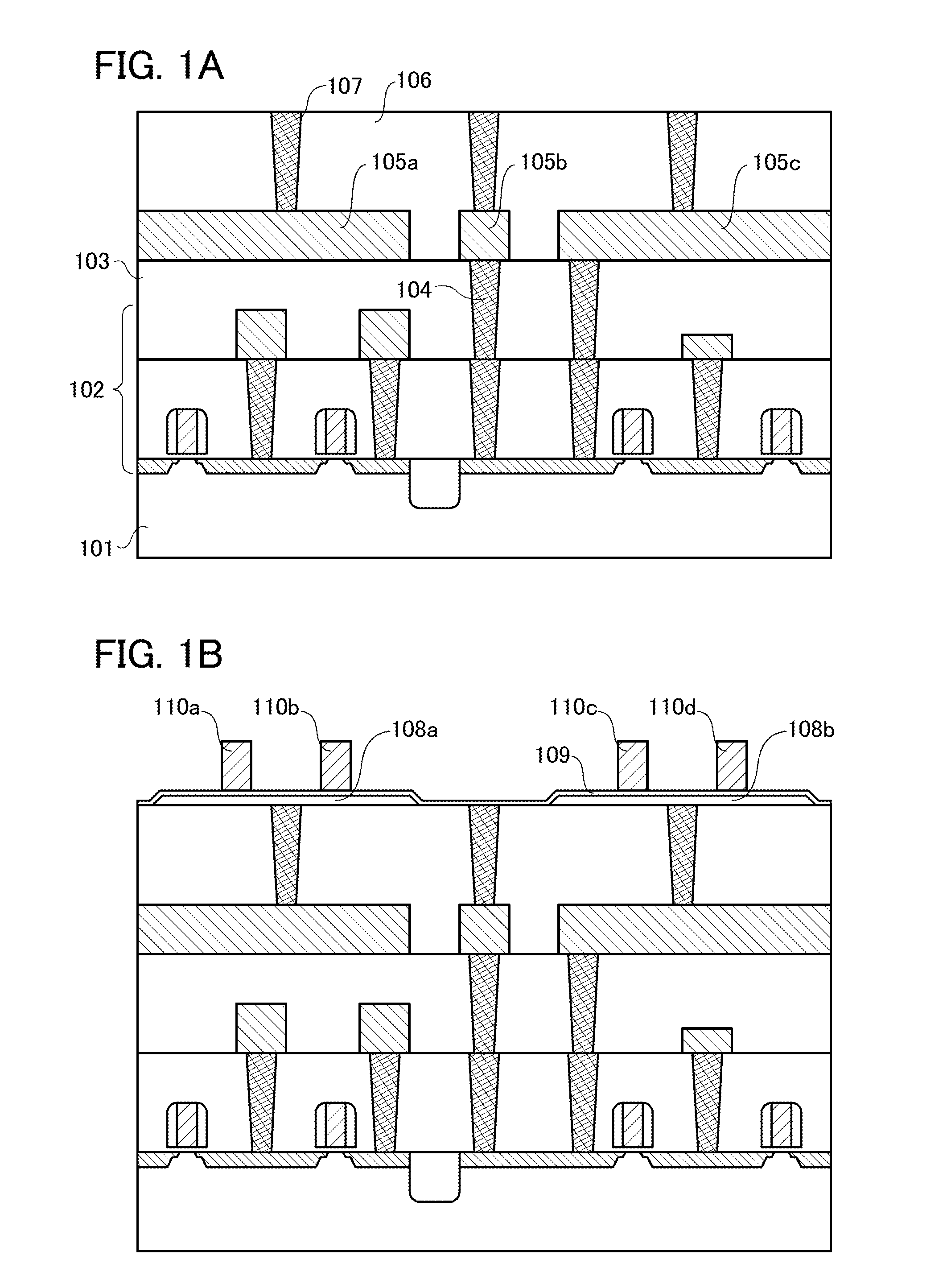
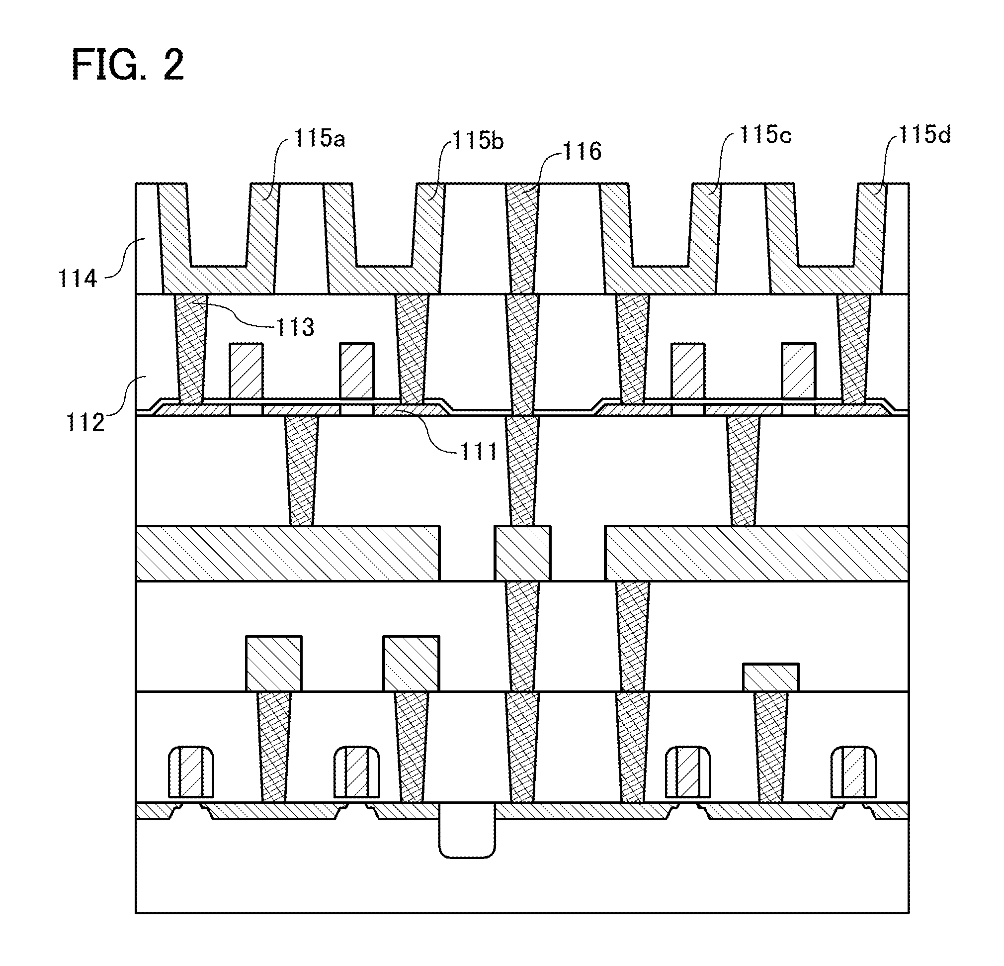
[0126]FIGS. 8A to 8D and FIGS. 9A to 9D illustrate this embodiment. Although in this embodiment, a memory cell is formed over a semiconductor circuit including a sense amplifier as in Embodiment 1, such a semiconductor circuit is omitted in FIGS. 8A to 8D and FIGS. 9A to 9D. Description is made below with reference to the drawings.

8A>

[0127]A sub bit line 402 is formed over a first insulator 401. At this time, there are some methods of arrangement of the sub bit line 402. For example, there is a method in which, as illustrated in FIGS. 9A and 9B, the sub bit line 402 and adjacent sub bit lines 402a and 402b are formed at the same depth or formed in the same layer. FIG. 9A is a schematic view of a cross section of a surface where the sub bit line 402 is formed, which is taken along a plane through line C-D of FIG. 8A, and FIG. 9B illustrates a cross section taken along line E-F of FIG. 9A. Note that cross sections along lines A-B of FIGS. 9A and 9C are illustrated in FIGS. 8A to 8D.

[0...


PUM


Abstract

The capacitance of a capacitor that is required in a DRAM is reduced, whereby a highly integrated DRAM is provided. In a divided bit line type DRAM, a sub bit line is formed below a word line and a bit line is formed above the word line. The parasitic capacitance of the sub bit line is reduced by employing the divided bit line method, and further, the off resistance of a cell transistor is set high according to need; thus, the capacitance can be one tenth or less of that of a conventional DRAM. Accordingly, even when a stacked capacitor is employed, the height of the capacitor can be one tenth or less of that of a conventional one, so that a bit line can be easily provided thereover. Further, by devising a structure of the cell transistor, the area per memory cell can be reduced to 4 F2.

Description

BACKGROUND OF THE INVENTION[0001]1. Field of the Invention[0002]The present invention relates to a semiconductor memory device.[0003]2. Description of the Related Art[0004]A DRAM whose memory cell includes one transistor (cell transistor) and one capacitor can be highly integrated, has no limit on the number of times of writing in principle, and can perform writing and reading at relatively high speed; thus, such a DRAM is used in many kinds of electronic appliances. Various efforts have been made to further increase the degree of integration of a DRAM (see Patent Document 1).[0005]A DRAM stores data by accumulating electric charge in a capacitor of each memory cell, and reads the data by releasing the electric charge to a bit line.[0006]The amount of change in the potential of the bit line due to the release of the electric charge is determined by the ratio between the capacitance of the capacitor and the parasitic capacitance of the bit line. The parasitic capacitance of the bit l...

Claims


Application Information

Patent Timeline
IPC IPC(8): G11C11/24
CPCG11C11/4097G11C11/404
Inventor TAKEMURA, YASUHIKO
Owner SEMICON ENERGY LAB CO LTD
Why Eureka
Try Eureka