Semiconductor device including current control function and self-interrupt function

a technology of current control and semiconductor, which is applied in the direction of pulse generator, pulse technique, lighting and heating apparatus, etc., can solve the problems of difficult to maintain a constant current, reducing the drain current id, and engine damage, so as to reduce the voltage range, reduce the duty, and avoid erroneous ignition

Inactive Publication Date: 2013-10-24
FUJI ELECTRIC CO LTD
View PDF7 Cites 5 Cited by
  • Summary
  • Abstract
  • Description
  • Claims
  • Application Information

AI Technical Summary

Benefits of technology

[0026]According to some embodiments, it is possible to control at least one of the voltage range or duration of one stage of the voltage whose amplitude is temporally changed in stages, and thus possible to control the current of the second semiconductor switching element as desired. For example, by lengthening the turn-on timing cycle, it is possible to lengthen the duration of one stage of the voltage whose amplitude is temporally changed in stages. Also, by reducing the duty, it is possible to reduce the voltage range of one stage of the voltage whose amplitude is temporally changed in stages. That is, it is possible to reliably prevent burning of the IGBT or ignition coil, and erroneous ignition, even when reducing the capacitance of the self-interrupting circuit capacitor.
[0027]The semiconductor device according to the aspect of the invention is such that the interval generator circuit lengthens the turn-on timing cycle of the third semiconductor switching element further the higher the temperature of a predetermined region.
[0028]According to some embodiments, it is possible to reduce variation in the amount of change in one stage of the voltage whose amplitude is temporally changed in stages caused by temperature change in a predetermined region. That is, it is possible to control the current of the second semiconductor switching element so that dependency on the temperature of a predetermined region is reduced.
[0029]The semiconductor device according to the aspect of the invention is such that the interval generator circuit reduces the duty of the third semiconductor switching element further the higher the voltage of the second capacitor.
[0030]According to some embodiments, the amount of change in one stage of the voltage whose amplitude is temporally changed in stages is such that the duration of the sudden voltage drop when the voltage across the self-interrupting circuit capacitor is high can be reduced, and the voltage range narrowed. That is, as it is possible to obtain a still gentler change in the current of the second semiconductor switching element, it is possible to more reliably prevent erroneous ignition.
[0031]According to the semiconductor device of the invention, an excellent advantage may be obtained in that it is possible to reliably prevent burning of an IGBT or ignition coil, and erroneous ignition, even when reducing the capacitance of a capacitor generating a self-interrupting circuit time constant.

Problems solved by technology

However, when the collector current Ic is abruptly interrupted using this kind of current control function or self-interrupt function, fluctuation is caused in the collector current Ic, and there is a problem in that erroneous ignition of a spark plug 4 is caused, and the engine is damaged.
However, as the drain current Id is an extremely low current in the order of nA, the more the drain current Id is reduced, the more difficult it becomes to maintain a constant current.
Consequently, reducing the drain current Id is not desirable.
Also, as erroneous ignition occurs when the inclination dlc / dt of the collector current is too large, while the IGBT or ignition coil L is burned when the inclination dlc / dt is too small, there is a demand for a high precision drain current Id control.
Thus, as described in the related art, there is a limit to the reduction of capacitance of the self-interrupting circuit capacitor and the accuracy of current control, as well as other shortcomings.

Method used


Image

  • Semiconductor device including current control function and self-interrupt function
  • Semiconductor device including current control function and self-interrupt function
  • Semiconductor device including current control function and self-interrupt function

Examples


first embodiment

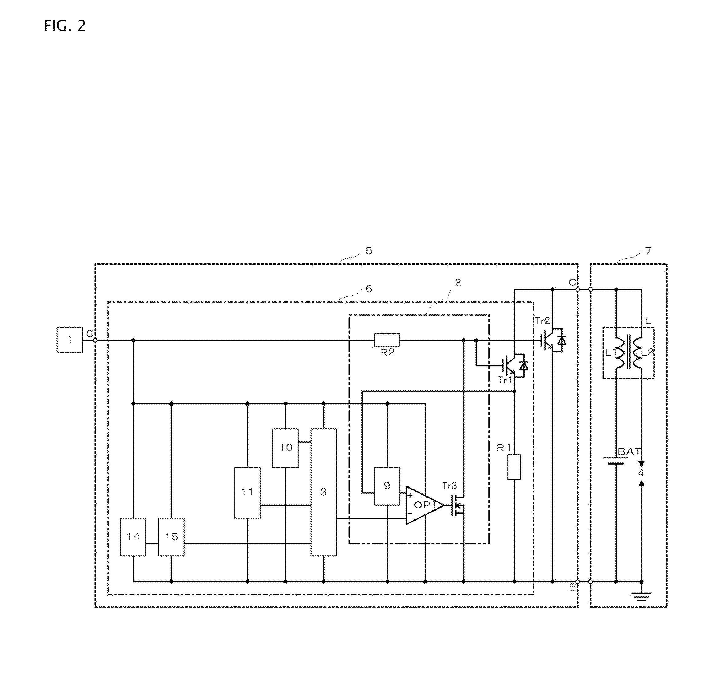
[0051]FIG. 2 shows a semiconductor device according to a first embodiment of the invention, wherein portions given the same reference signs as in FIG. 17 represent the same portions, and the basic configuration is the same as the heretofore known configuration shown in FIG. 17.

[0052]Next, a description will be given of a circuit configuration of the first embodiment.

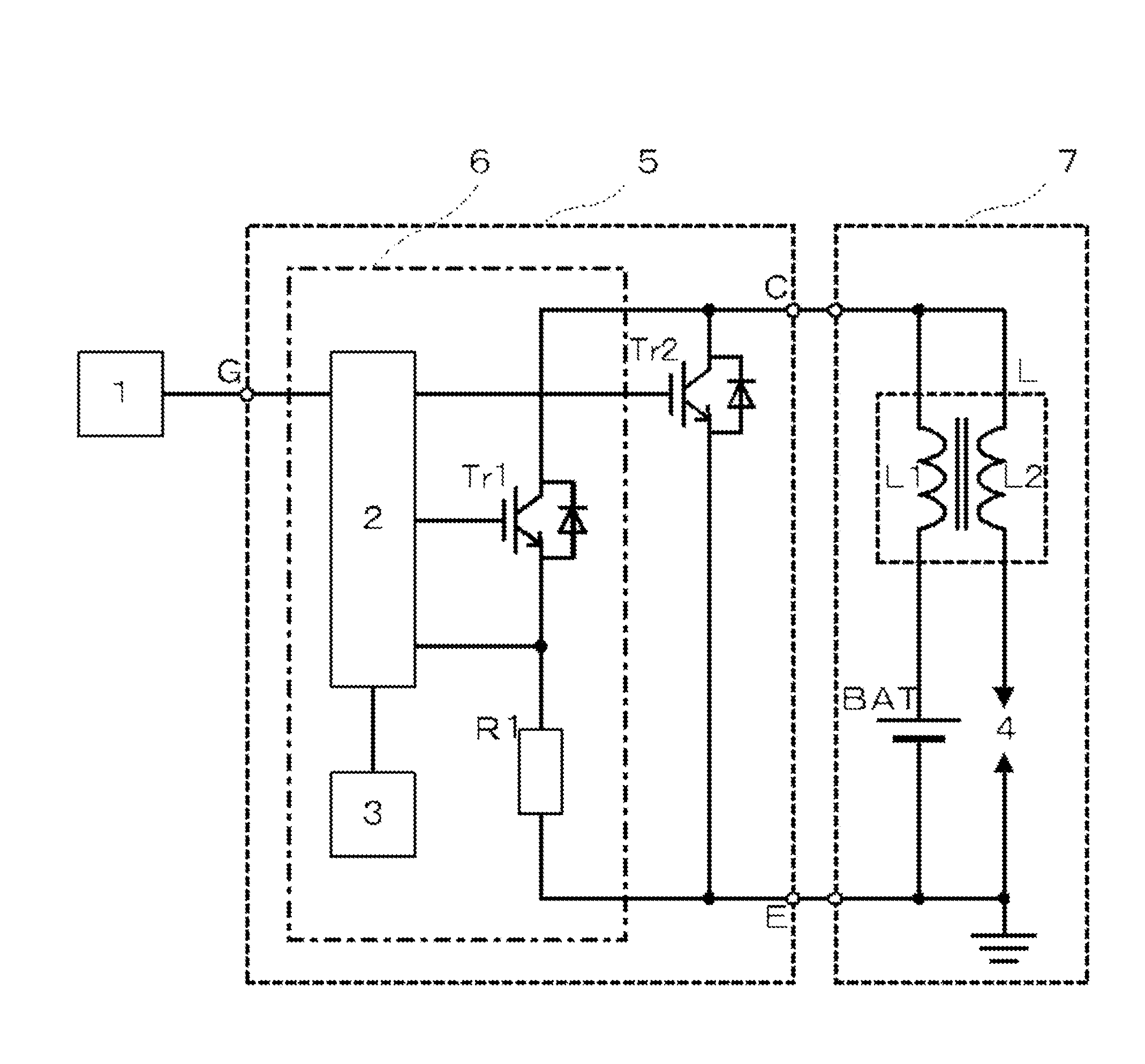
[0053]The circuit of the first embodiment of the invention is configured of an ECU 1, a semiconductor device 5, and an ignition unit 7. The semiconductor device 5 has a G terminal, a C terminal, and an E terminal, wherein the G terminal is connected to the ECU 1, and the C and E terminals are connected to the ignition unit 7.

[0054]The semiconductor device 5 is configured of an IGBT Tr2 and a current control circuit 6. The current control circuit 6 is configured of a first series circuit wherein an IGBT Tr1 and a sense resistor R1 are connected in series, a reference voltage supply 14, a level shift circuit 15, a drive si...

second embodiment

[0072]FIG. 6 shows a semiconductor device according to a second embodiment of the invention, wherein the basic configuration is the same as that of the first embodiment shown in FIG. 2. The circuit of the second embodiment of the invention has a timer circuit 12 and a pulse generator circuit 11 in addition to the circuit configuration of the first embodiment.

[0073]FIG. 7 shows circuit configuration examples for the timer circuit 12 and pulse generator circuit 11. The timer circuit 12 is configured of an oscillator 18, a reset circuit 19, and TFFs 20 to 29. The TFFs 20 to 29 are connected in a ten stage series, wherein the output of the previous stage is connected to the input of the next stage.

[0074]The pulse generator circuit 11 has MOSs Tr10 to Tr13 connected to each other in parallel. The pulse generator circuit 11 also has a sixth series circuit, wherein the source of a DepMOS Tr15 and the drain of the MOS Tr13 are connected, the MOS Tr14 are connected. Also, the sixth series ci...

third embodiment

[0081]FIG. 9 shows a semiconductor device according to a third embodiment of the invention, wherein the basic configuration is the same as that of the second embodiment shown in FIG. 6. The circuit of the third embodiment of the invention has a temperature compensation circuit 13, a constant current source 34, a level shift circuit 35, and a diode D. in addition to the circuit configuration of the second embodiment.

[0082]FIG. 10 shows a circuit configuration example for the temperature compensation circuit 13. The temperature compensation circuit 13 has voltage dividing resistors R3 to R5 connected in series between the G terminal and E terminal, and comparators COMP1 and COMP2. An overheat detection voltage is input into the negative side terminals of the comparators COMP1 and COMP2, while voltages V1 and V2, wherein the voltage between the G terminal and E terminal is divided by the voltage dividing resistors R3 to R5, is input into the positive side terminals. Herein, the forward...


PUM


Abstract

In aspects of the invention, there is provided an igniting semiconductor device that can prevent burning of an IGBT or ignition coil, and erroneous ignition, even when reducing the size of a capacitor that generates a self-interrupting circuit time constant. In some aspects, a semiconductor device of the invention is configured of an IGBT and a current control circuit. The current control circuit can be configured of a first series circuit wherein an IGBT and a sense resistor are connected in series, a drive signal control circuit, and a self-interrupting circuit. At a time of abnormal operation, the self-interrupting circuit can output a voltage whose amplitude temporally drops in stages toward 0V to the drive signal control circuit. The drive signal control circuit can control the amplitude of a drive control signal so that the voltage across the sense resistor is equivalent to the output voltage of the self-interrupting circuit.

Description

BACKGROUND OF THE INVENTION[0001]1. Technical Field[0002]Embodiments of the invention relate to semiconductor devices used in automobile internal combustion engine ignition devices, as well as other devices.[0003]2. Related Art[0004]FIG. 17 shows an example of a configuration of a heretofore known general internal combustion engine ignition semiconductor device using an insulated gate bipolar transistor (hereafter referred to as an IGBT) as a power semiconductor element. See, for example, Japanese Patent Application No. JP-A-2012-36848.[0005]An ignition device shown in FIG. 17 is configured of an engine control unit (hereafter referred to as an ECU) 1, a semiconductor device 5, and an ignition unit 7.[0006]The ignition device shown in FIG. 17 is such that, on an abnormal condition being detected, a self-interrupt signal Vsd is emitted from a self-interrupt signal source 10, a self-interrupting circuit 33 operates, and a collector current Ic of an IGBT Tr2 is interrupted. An abnormal...

Claims


Application Information

Patent Timeline
Patent Type & Authority Applications(United States)
IPC IPC(8): F02P3/00
CPCF02P3/00H03K4/023H03K17/0822H03K2017/0806F02P3/0554F02P3/04
Inventor YAMADA, KAZUHITO
Owner FUJI ELECTRIC CO LTD
Why Eureka
Try Eureka