
Compound Semiconductor Device on Virtual Substrate

a semiconductor and virtual substrate technology, applied in the field of semiconductor/solid-state device manufacturing, semiconductor/solid-state device layout, semiconductor devices, etc., can solve the problems of high defect density, mechanical strain in epitaxial film, and mismatch between substrates

Inactive Publication Date: 2012-09-06
POWER PHOTONICS +1
View PDF6 Cites 14 Cited by
  • Summary
  • Abstract
  • Description
  • Claims
  • Application Information

AI Technical Summary

Benefits of technology

[0028]In a fourth aspect of the present invention, an opportunity is provided to the skilled device designer to select, given the desired cut-off wavelength, the active

Problems solved by technology

In addition to the substrate crystal quality, the important parameter affecting the result is the lattice mismatch between the substrate and the epitaxially deposited film.
Large mismatch leads to the mechanical strain in the epitaxial film, which in turn is relaxed through the development of structural defects as the film thickness increases.
Bulk crystals are typically obtained by methods other than epitaxial deposition and are in most cases limited to binary compounds of the Group III and Group V elements.
These thicknesses are well above the critical thickness for strain relaxation in the strained crystalline film, so that epitaxial growth of these compounds on the lattice mismatched substrate results in high defect density developed due to the said strain relaxation.
Unfortunately, most of the compound semiconductors have high unintentional doping level, making depletion-based photodetection a challenging task.
However, the performance of these devices is currently limited by the absence of lattice-matched substrates that would allow fabrication of not strained and not relaxed light absorption layers of the thickness in micrometer scale (from about 0.1 micrometer to tens of micrometers).
Aluminum Antimonide AlSb and Gallium Antimonide GaSb bulk crystals are provided as available substrates, thus limiting the active region to a very narrow range of compositions.
While grown on GaAs substrates, such materials require larger lattice mismatch accommodations that cannot be achieved by monotonic composition grading due to the accumulated stress relaxation through structural defect development in the grown films.
First of all, the method of U.S. Pat. No. 7,633,083 is extremely complicated, as it requires precisely controlled growth of variable compounds comprising the transitional layer, of total thicknesses up to 10 micrometers, which is hard to achieve technologically.
Second, it ultimately requires high and variable Al compositions in the transitional layer.

Method used


Image

  • Compound Semiconductor Device on Virtual Substrate
  • Compound Semiconductor Device on Virtual Substrate
  • Compound Semiconductor Device on Virtual Substrate

Examples


Embodiment Construction

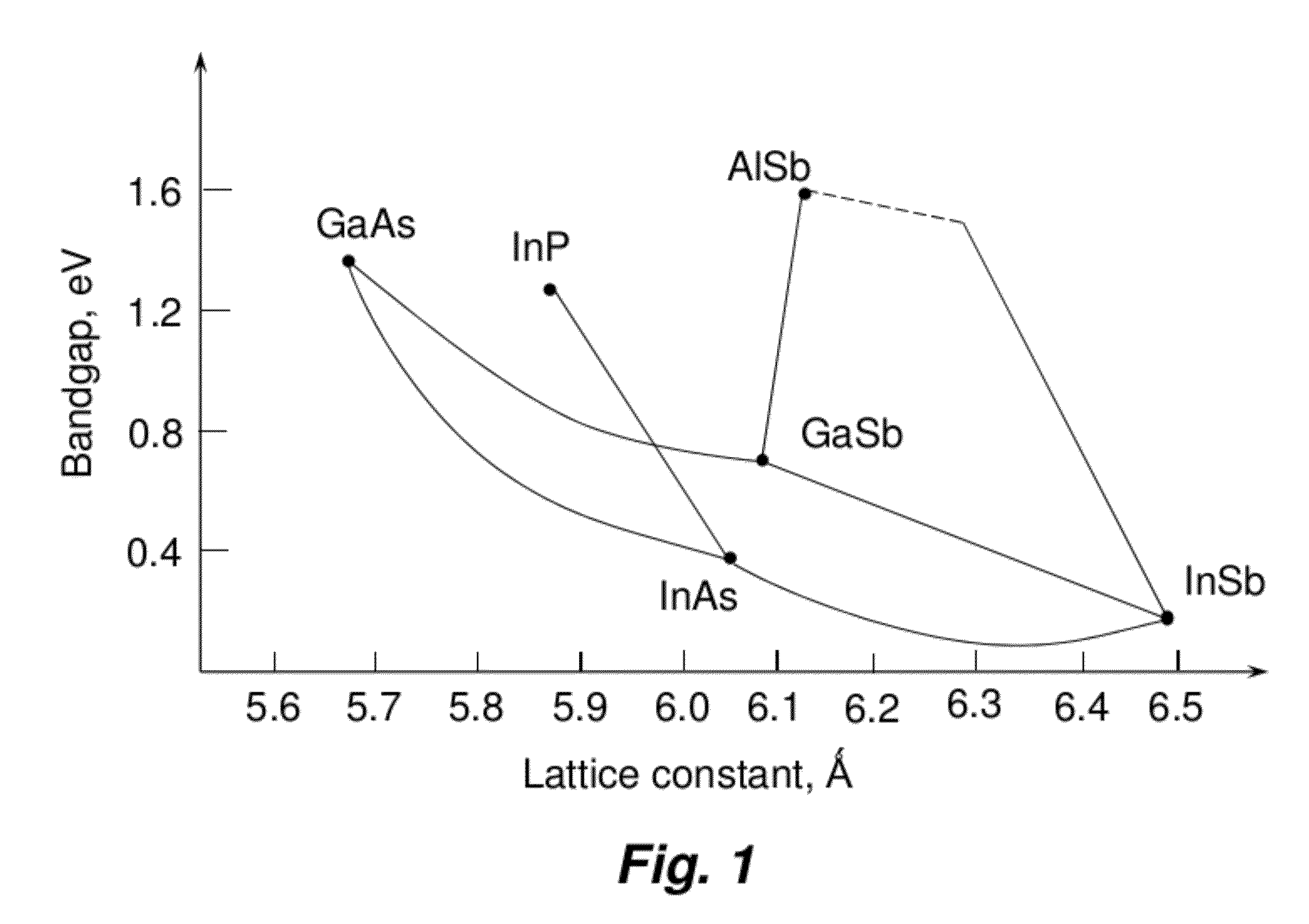
[0037]FIG. 1 presents the diagram showing the bandgaps of the narrow-band III-V compounds and their respective lattice constants. The lowest possible bandgap and largest associated wavelength are achieved for the compounds with the lattice constants around 6.3 Angstrom, which has no matching binary point. At the same time, the use of GaAs as a substrate, as in the Prior Art, is definitely not optimal due to much larger lattice mismatch than, for example, for GaSb and InSb.

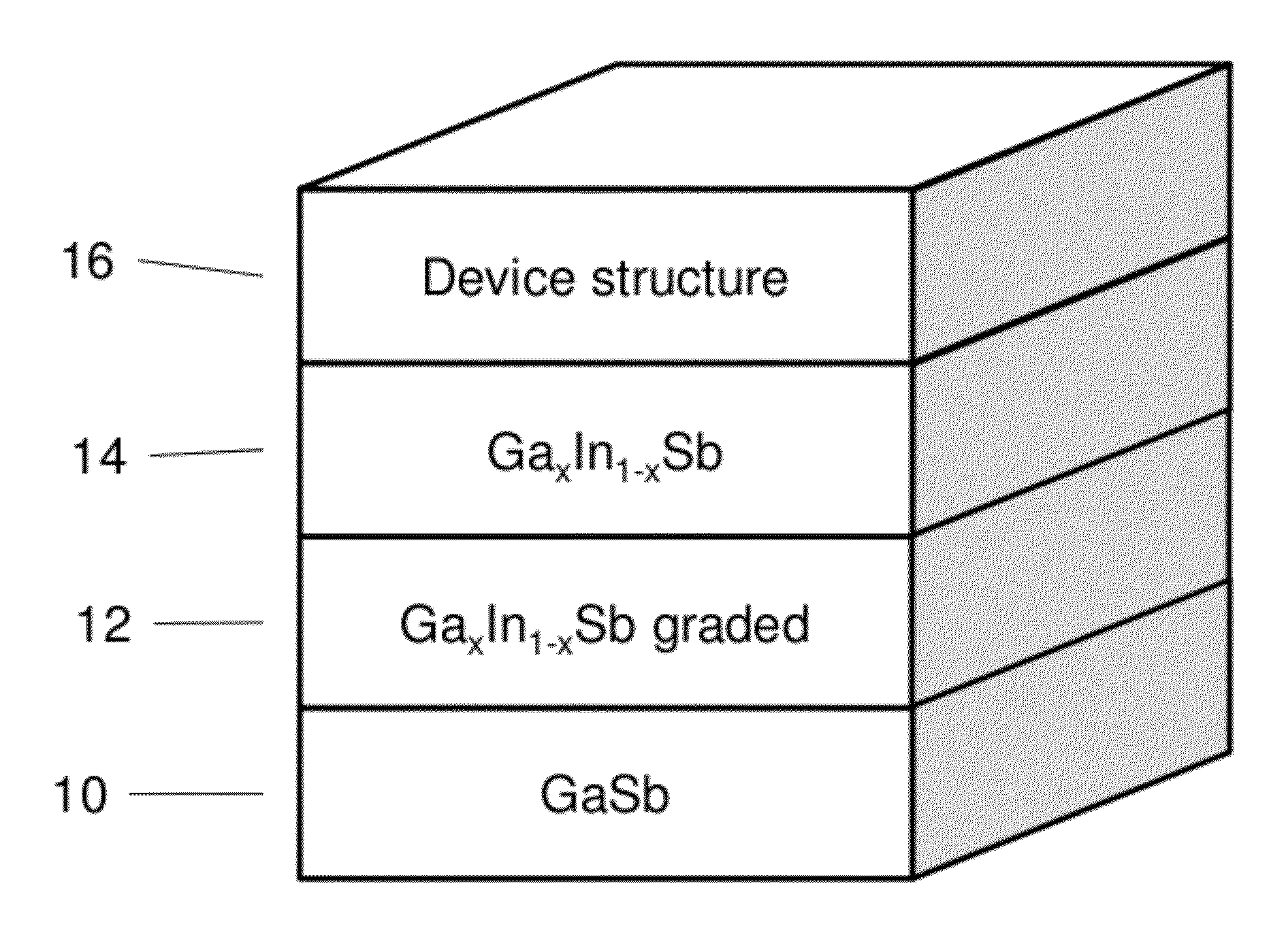
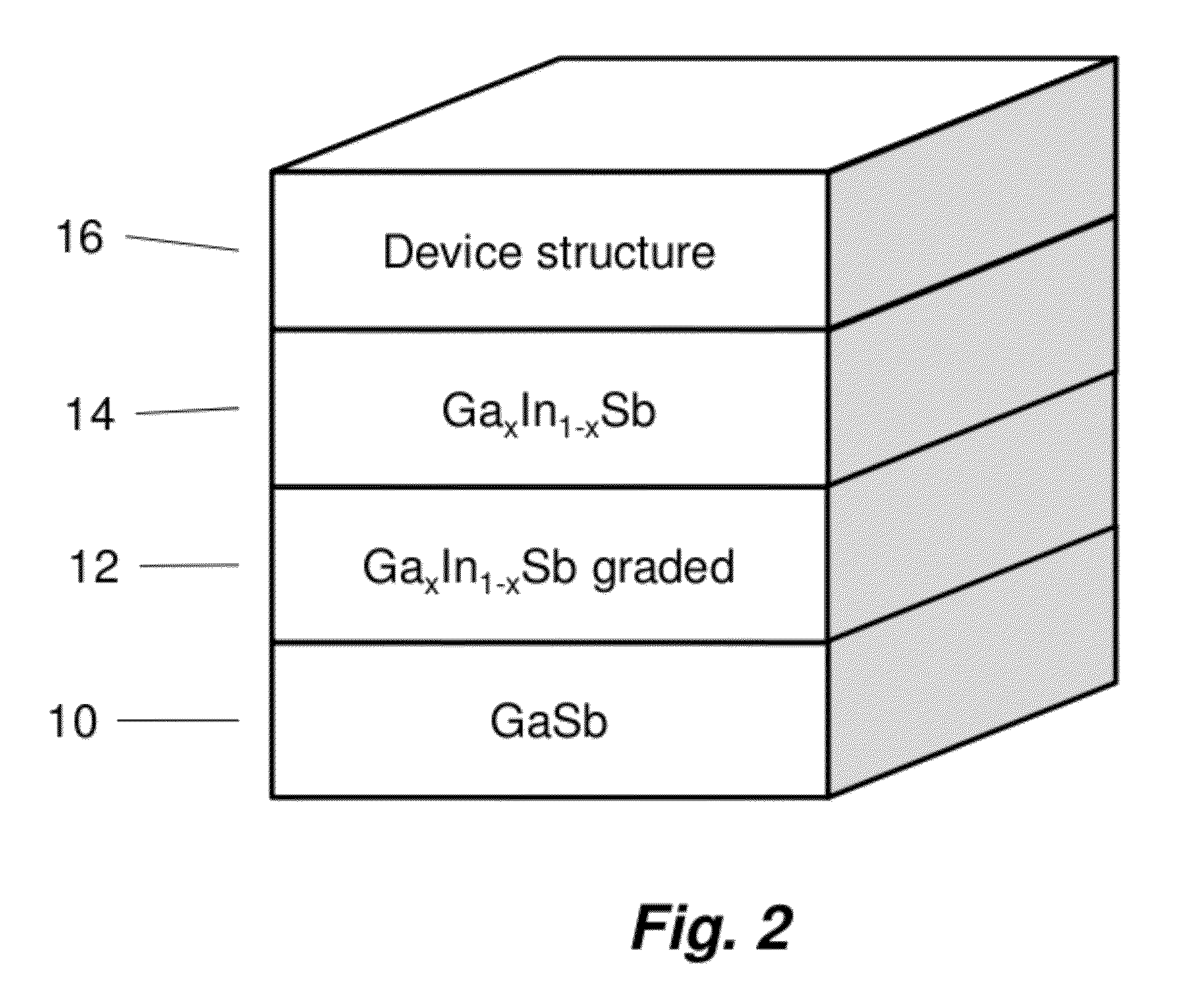
[0038]FIG. 2 illustrates one of the semiconductor device structures according to the present invention. The device structure is optimized for the active layer having the lattice constant between approximately 6.1 and 6.3 Angstrom. According to the teaching of the present invention, this can be achieved by obtaining, for example, bulk GaSb substrate 10 (commercially available in qualities suitable for the epitaxial growth); growing on its surface by means of MBE or MOVPE the graded transitional layer 12 of GaInAsSb ...


PUM


Abstract

A method of fabrication of barrier diode based infrared detectors, utilizing the growth of unstrained, not relaxed III-V compound semiconductor material layers having a lattice constant over 6 Angstrom, is provided. The growth is performed by the means of Molecular Beam Epitaxy (MBE) or Metal-Organic Vapor Phase Epitaxy (MOVPE). The method comprises the use of bulk crystalline substrates and the growth of a transitional layer of GaInAsSb with graded composition, followed by an optional thick layer of GaInAsSb of constant composition, lattice matched to the said III-V compound semiconductor material layers, the said optional layer of GaInAsSb of constant composition serving as a virtual substrate. The method provides high crystalline quality layers suitable for semiconductor device fabrication that can effectively interact with electromagnetic radiation of the mid-infrared spectral range with a wavelength between about 2 micrometers to about 16 micrometers.

Description

CROSS-REFERENCE TO RELATED APPLICATION [0001]Not ApplicableFEDERALLY SPONSORED RESEARCH [0002]Not ApplicableSEQUENCE LISTING OR PROGRAM [0003]Not ApplicableFIELD OF THE DISCLOSURE[0004]Aspects of the invention relate generally to solid state detectors of electromagnetic radiation in the mid-infrared spectral range, and more particularly, to semiconductor devices fabricated from compound alloys comprising the elements of Group III and Group V of the Periodic System of Elements by means of Molecular Beam Epitaxy and Metal-Organic Vapor Phase Epitaxy.BACKGROUND OF THE DISCLOSURE[0005]Solid state electronic devices efficiently interacting with the electromagnetic radiation of various spectral ranges are the basis of state-of-the-art communications, space and other emerging technologies. This rapidly growing market became available due to the effects of electron-hole pair generation and recombination in the semiconductor materials. The most practical material system for these optoelectro...

Claims


Application Information

Patent Timeline
IPC IPC(8): H01L31/0304
CPCY02E10/544H01L31/06875H01L31/03046H01L31/101
Inventor BELENKY, GREGORYSHTERENGAS, LEONWESTERFELD, ARTHUR DAVID
Owner POWER PHOTONICS
Learn More