

Light emitting element, light source device, and projection display device
- Summary
- Abstract
- Description
- Claims
- Application Information
AI Technical Summary
Benefits of technology
Problems solved by technology
Method used
Image

Examples
first embodiment
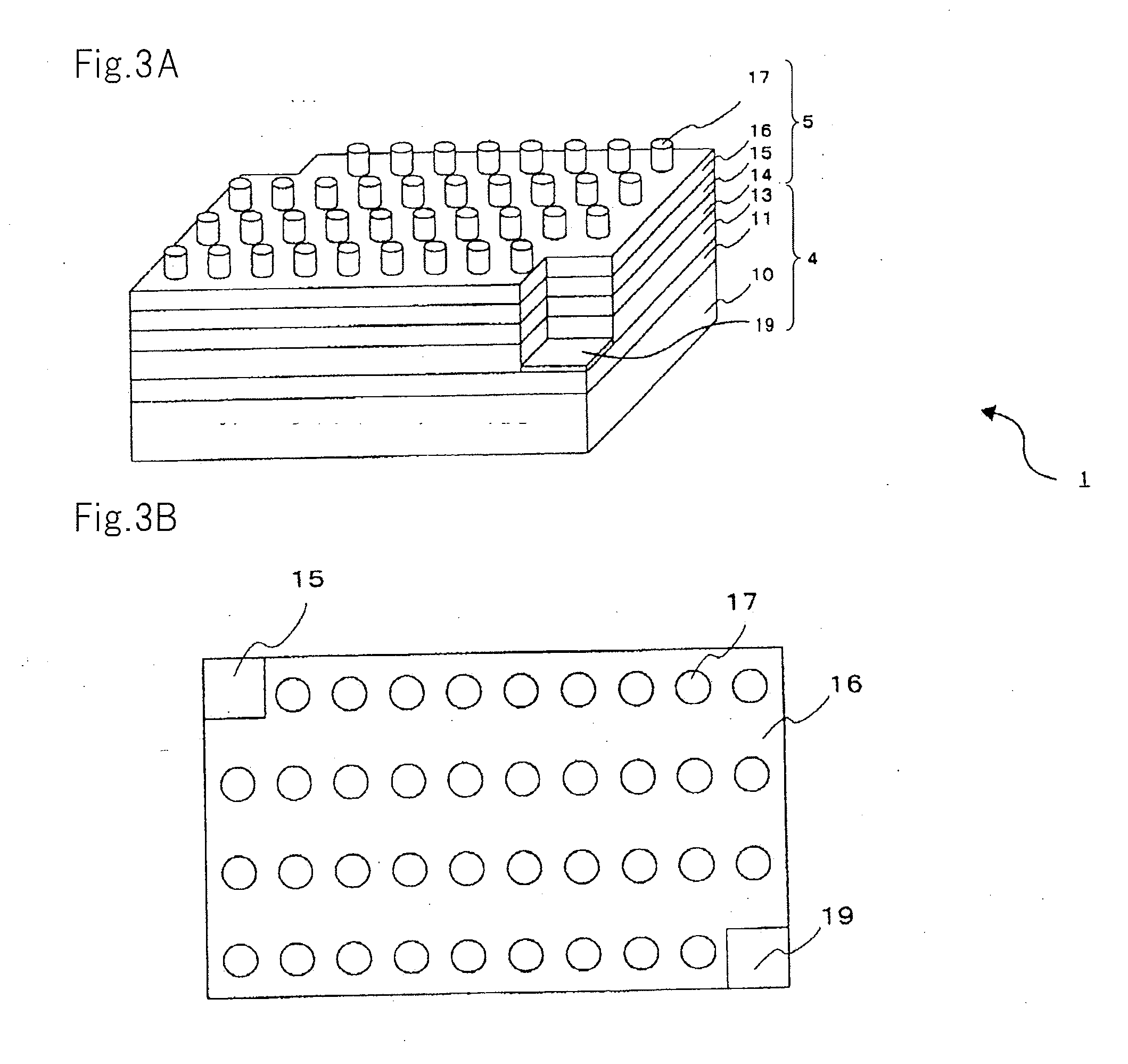
[0062]FIG. 3A is a perspective view schematically showing a configuration of a light emitting element according to a first embodiment. FIG. 3B is a plan view schematically showing the configuration of the light emitting element according to the first embodiment. In the light emitting element, individual layers are actually very thin, and there is a large difference in thickness among the layers. It is therefore difficult to draw the layers in accurate scale and proportion. Thus, in the drawings, the layers are not drawn in actual proportion, but are shown schematically.
[0063]As shown in FIG. 3A, light emitting element 1 according to the first embodiment includes light source layer 4, and directional control layer 5 that is stacked on light source layer 4 and that serves as an optical element layer, into which light from light source layer 4 enters.
[0064]Light source layer 4 includes substrate 10 and a pair of layers, namely, hole-transport layer 11 and electron-transport layer 13, f...
second embodiment
[0101]FIG. 4A is a perspective view schematically showing a light emitting element according to a second embodiment. FIG. 4B is a plan view schematically showing the light emitting element according to the second embodiment.
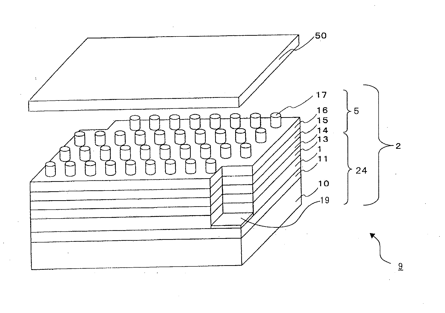
[0102]As shown in FIGS. 4A and 4B, light emitting element 2 according to the second embodiment includes light source layer 24, and directional control layer 5 that is stacked on light source layer 24 and that serves as an optical element layer, into which light from light source layer 24 enters. Directional control layer 5 included in light emitting element 2 of the second embodiment is similar to that of the first embodiment, and thus description thereof is omitted.
[0103]Light source layer 24 included in light emitting element 2 of the second embodiment is different from light source layer 4 of the first embodiment in that active layer 12 is formed between hole-transport layer 11 and electron-transport layer 13.
[0104]For active layer 12 of light source layer 24,...
third embodiment
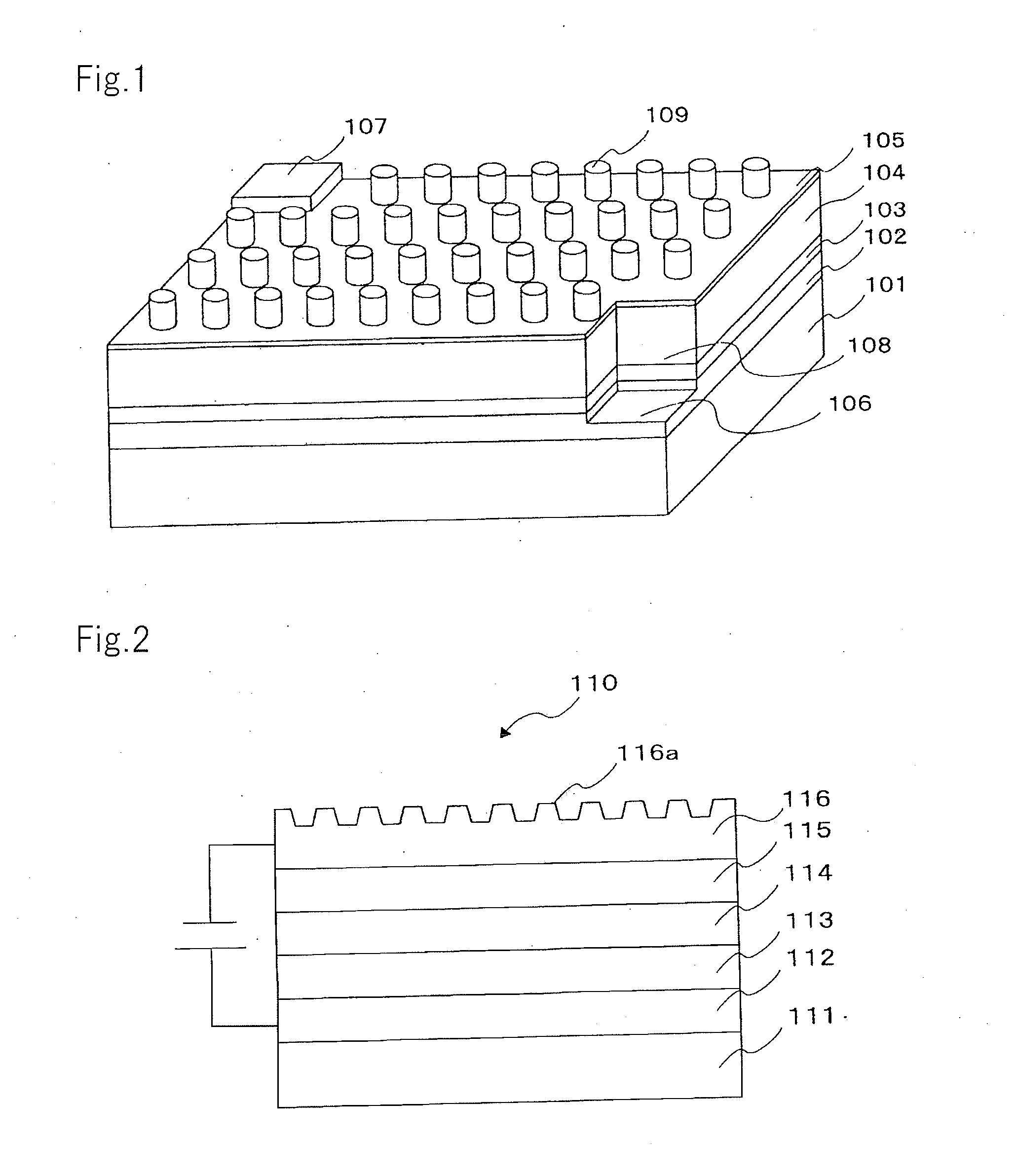
[0110]FIG. 7A is a perspective view schematically showing a light emitting element according to a third embodiment. FIG. 7B is a plan view schematically showing the light emitting element according to the third embodiment.
[0111]As shown in FIGS. 7A and 7B, light emitting element 3 according to the third embodiment includes light source layer 34, and directional control layer 5 that is stacked on light source layer 34 and that serves as an optical element layer, into which light from light source layer 34 enters. Directional control layer 5 included in light emitting element 3 of the third embodiment is similar to that of the first embodiment, and thus description thereof is omitted. Light source layer 34 included in light emitting element 3 of the third embodiment is different from light source layer 24 of the second embodiment in that anode layer 29 that serves as an anode is formed on the entire surface of substrate 10 between substrate 10 and hole-transport layer 11.
[0112]In the ...
PUM
 Abstract
Description
Claims
Application Information