Defect inspection device and defect inspection method

Active Publication Date: 2012-09-13
HITACHI HIGH-TECH CORP
View PDF4 Cites 60 Cited by
  • Summary
  • Abstract
  • Description
  • Claims
  • Application Information

AI Technical Summary

Benefits of technology

[0015]The invention disclosed in the present application provides the defect inspection device and defect inspection

Problems solved by technology

However, the judgment with the low threshold entails the detection of a large number of false defects attributable to sampling erro

Method used


Image

  • Defect inspection device and defect inspection method
  • Defect inspection device and defect inspection method
  • Defect inspection device and defect inspection method

Examples


Example

First Embodiment

[0043]A defect inspection technique (defect inspection method and defect inspection device) according to a first embodiment of the invention will be described in detail as below.

[0044]A pattern inspection technique according to the first embodiment of the invention is described by way of example of a defect inspection device and defect inspection method using dark field illumination of a semiconductor wafer as an inspection object.

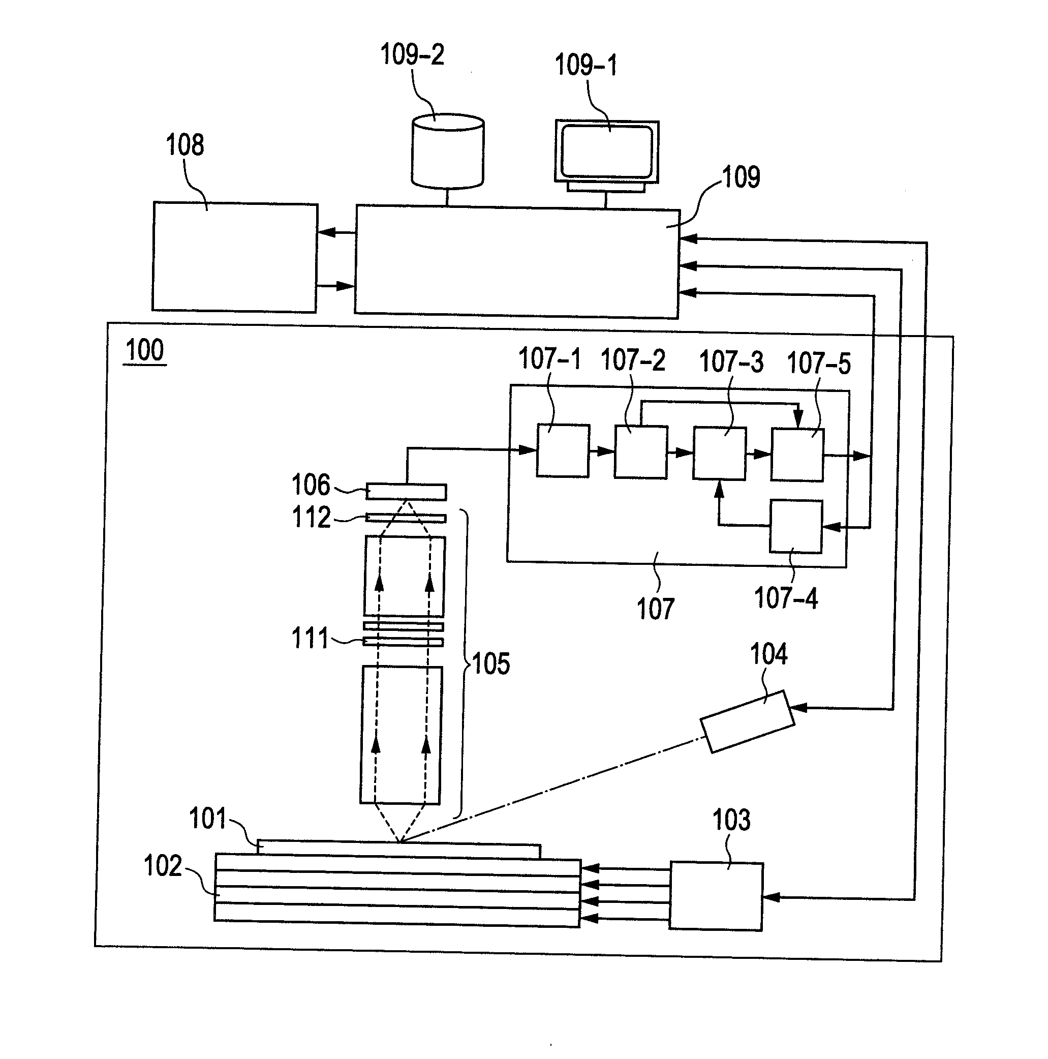
[0045]FIG. 1 shows an exemplary arrangement of a defect inspection device using dark field illumination according to the first embodiment. The defect inspection device of the first embodiment includes a defect candidate detection unit 100, a post-inspection processing unit 108 and a main control unit 109 (including a user interface 109-1 and a recording unit 109-2).

[0046]The defect candidate detection unit 100 includes a stage 102, a mechanical controller 103, an illumination optical system (illumination unit) 104, a detection optical syste...

Example

Second Embodiment

[0119]Next, another embodiment of the defect inspection device including the image processing system having the above-described system structure is described by way of example where the inspection device includes a plurality of illumination optical systems and detection optical systems for image detection.

[0120]FIG. 13 is a diagram showing an exemplary arrangement of a defect inspection device according to a second embodiment of the invention. The figure shows an example where the defect inspection device using the dark field illumination shown in FIG. 1 is provided with two illumination optical systems and two detection optical systems. The device includes: illumination optical systems 104-1, 104-2; an upper detection system (detection optical system) 105-1; an oblique detection system (detection optical system) 105-2; and image sensors 106-1, 106-2. The defect inspection device further includes an image comparison processing unit 107 (preprocessing unit 107-1, ima...

Example

Third Embodiment

[0122]Still another embodiment of the defect inspection device including the image processing system having the above-described structure is described by way of example where the inspection device includes an optical system capable of illuminating light having multiple wavelengths, and detection optical systems that can receive discrete lights having different wavelengths respectively.

[0123]FIG. 14 is a diagram showing an exemplary arrangement of a defect inspection device according to a third embodiment of the invention. The figure illustrates an example where the defect inspection device using the dark field illumination shown in FIG. 1 is provided with an illumination optical system capable of illuminating light having different wavelengths and detection optical systems that can receive discrete lights having different wavelengths respectively. An illumination unit 104-3 illuminates the sample 101 with light having different wavelengths (e.g., λ1, λ2). Scattered l...


PUM


Abstract

Disclosed is a defect inspection device that has an illumination optical system; a detection optical system; and a processing unit which includes a defect feature quantity calculation unit that calculates the feature quantities of each defect candidate, a defect candidate grouping unit that groups the aforementioned defect candidates on the basis of the feature quantities, a defect classification evaluation value calculation unit that calculates defect classification evaluation values for the aforementioned defect candidates, a defect classification evaluation value updating unit that, on the basis of instructions, updates the evaluation values, a defect classification threshold determination unit that, on the basis of evaluation valued updated by the aforementioned defect classification evaluation value updating unit, determines a classification boundary that is a threshold for classifying defect types of the aforementioned defect candidates, and a defect detection unit that detects defects using the thresholds.

Description

TECHNICAL FIELD[0001]The present invention relates to a defect inspection device and defect inspection method for high-sensitivity inspection of microscopic defects present on a sample surface.BACKGROUND ARTS[0002]Thin-film devices such as semiconductor wafers or for use in liquid crystal displays and magnetic heads for hard disk drives are fabricated through a large number of processing steps. In the fabrication of such a thin-film device, an appearance inspection is performed at the end of each of process flows for the purpose of yield improvement and consistent production. In the appearance inspection, a pattern defect or a defect such as foreign substance is detected based on a reference image and an inspection image obtained by illuminating a region with lamp light, laser, electron beam or the like, the region corresponded by two patterns which are to be fundamentally formed in the same configuration. More specifically, the reference image and inspection image are registered wi...

Claims


Application Information

Patent Timeline
IPC IPC(8): G06K9/60H04N7/18
CPCG01N21/9501G01N2021/8825G01N2021/9513G06T7/0004G01N21/95607G06T2207/30121G06T2207/30148H01L22/12G06T2207/10061
Inventor URANO, TAKAHIROSAKAI, KAORUHONDA, TOSHIFUMI
Owner HITACHI HIGH-TECH CORP
Why Eureka
Try Eureka