Semiconductor light emitting device and manufacturing method

a technology of semiconductors and light-emitting devices, which is applied in the direction of solid-state devices, transportation and packaging, lighting and heating apparatus, etc., can solve the problems of difficult to reduce the size of the light-emitting surface is difficult to meet the requirements of the lead frame type light-emitting device, and the effect of high light-emitting efficiency

Inactive Publication Date: 2012-09-20
STANLEY ELECTRIC CO LTD
View PDF2 Cites 110 Cited by
  • Summary
  • Abstract
  • Description
  • Claims
  • Application Information

AI Technical Summary

Benefits of technology

[0041]According to the exemplary manufacturing method described above for the semiconductor light-emitting devices, the side slant or inclined surface and the convex surface of the reflective material layer used as the reflector can be formed by disposing an uncured reflective material between the frame and the side surfaces of the wavelength converting layer and the optical plate and between both the bottom surface of each of the light-emitting chips and the at least one concave surface of the wavelength converting layer and the mounting surface of the base board. The wavelength converting layer and the reflective material layer can be solidified by a similar method as compared to conventional processes. Thus, the method can provide semiconductor light-emitting devices having various small light-emitting surfaces, a high light-emitting efficiency and a substantially uniform color tone using manufacturing machines that are similar to those used to manufacture conventional semiconductor light-emitting devices.

Problems solved by technology

Accordingly, it may be difficult for the lead frame type light-emitting device 20 to reduce the size of a light-emitting surface because the light expands from the cavity 27.
Additionally, the radial type light-emitting device 30 may emit a wavelength-converted light in a radial fashion from the casing 36, and therefore may also be difficult to reduce the size of a light-emitting surface.
Therefore, the semiconductor light-emitting devices including the cavities disclosed in Patent Documents No. 1 to No. 4 may not be a match for the above-described usage, and also the radial type light-emitting devices disclosed in Patent Document No. 1 and No. 5 may not be a match for the usage.

Method used


Image

  • Semiconductor light emitting device and manufacturing method
  • Semiconductor light emitting device and manufacturing method
  • Semiconductor light emitting device and manufacturing method

Examples


Embodiment Construction

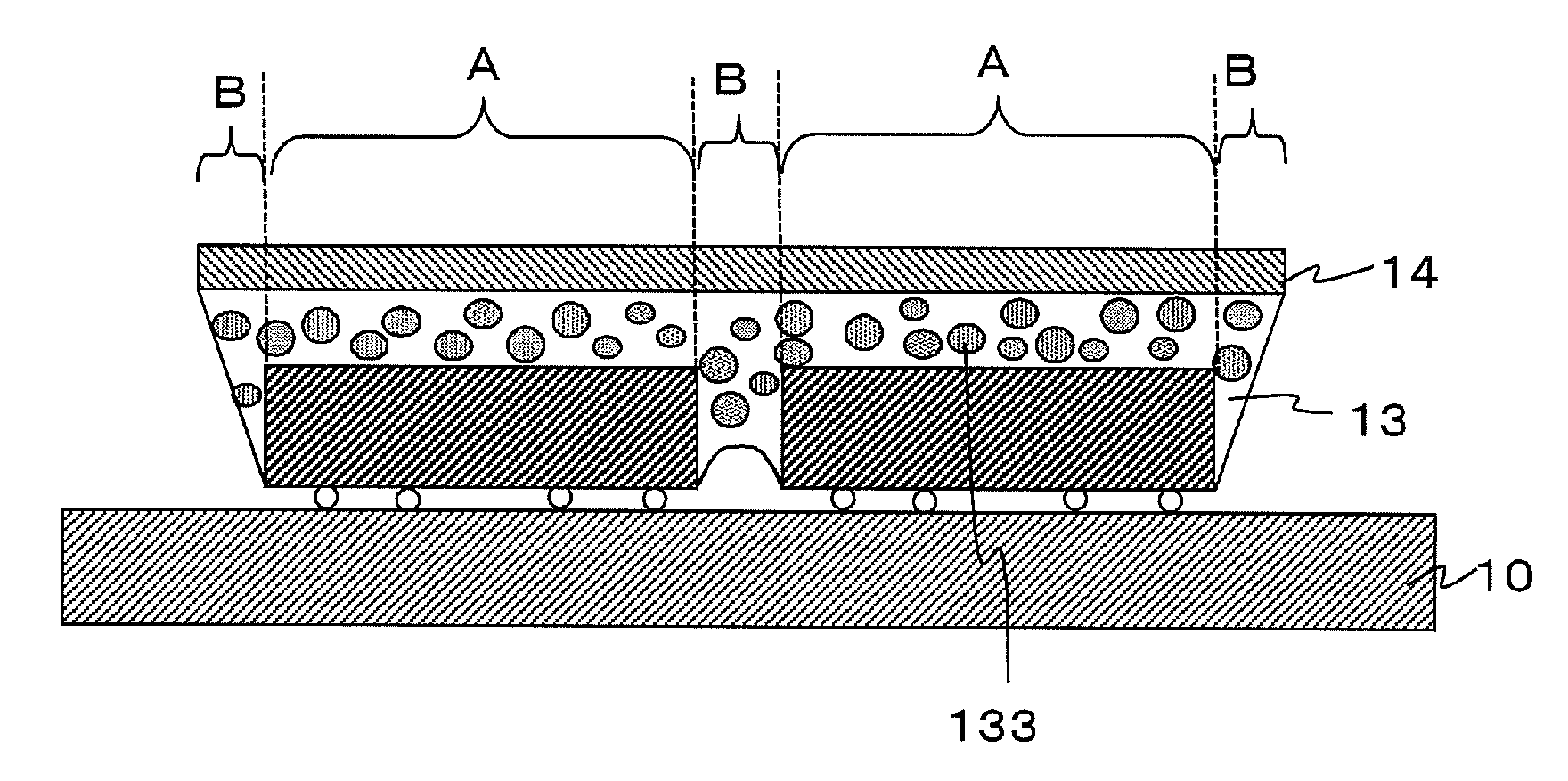
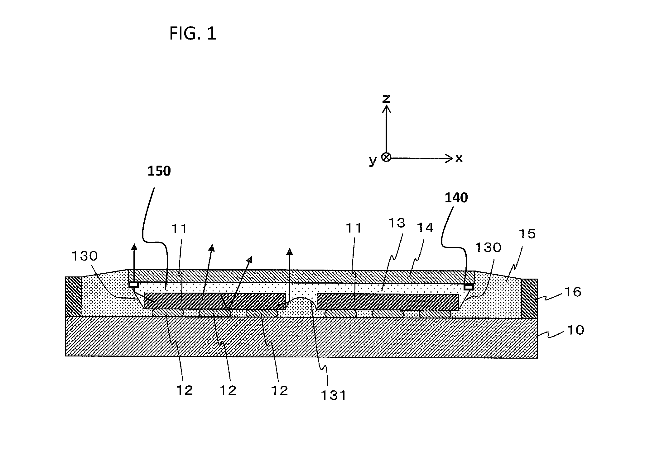
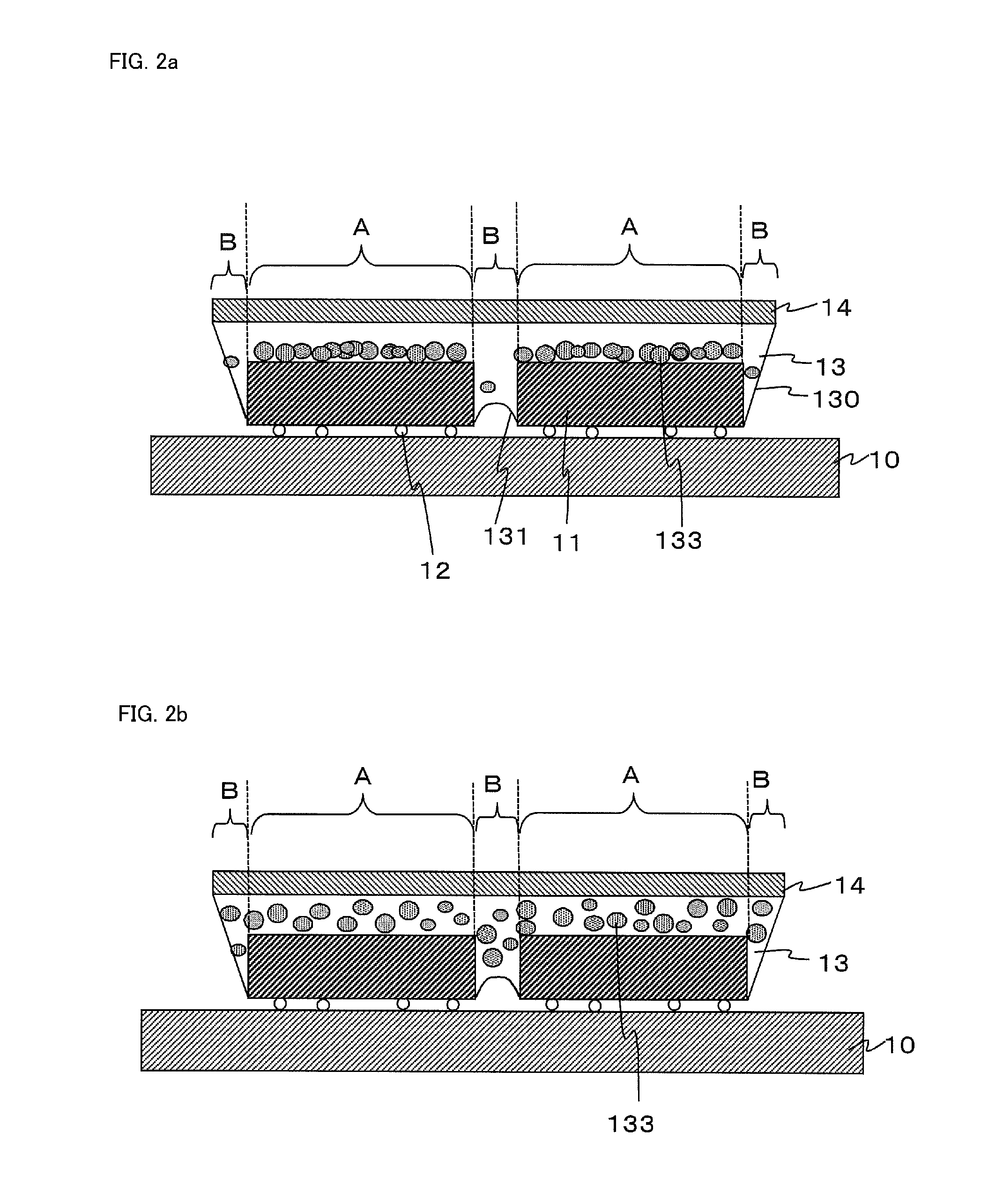
[0050]Exemplary embodiments and manufacturing methods of the disclosed subject matter will now be described in detail with reference to FIGS. 1 to 5b. FIG. 1 is an enlarged side cross-sectional view showing an exemplary embodiment of a semiconductor light-emitting device made in accordance with principles of the disclosed subject matter.

[0051]The semiconductor light-emitting device can include a base board 10 having a mounting surface and a conductor pattern (not shown in FIG. 1) formed on the mounting surface, and a plurality of semiconductor light-emitting chips 11 having an outside surface and at least one pair of adjacent surfaces located between the adjacent light-emitting chips, each of the light-emitting chips 11 having a top surface and a bottom surface and including chip electrodes adjacent the bottom surface.

[0052]Each of the chip electrodes can be mounted on the mounting surface of the base board 10 via solder bumps 12 and can be electrically connected to a respective por...


PUM


Abstract

A semiconductor light-emitting device and a method for manufacturing the same can include a wavelength converting layer in order to emit various colored lights including white light. The device can include a board, a frame located on the board, at least one light-emitting chip mounted on the board, the wavelength converting layer located between an optical plate and an outside surface of the chips so that a density of a peripheral region is lower than that of a middle region, and a reflective material layer disposed at least between the frame and a side surface of the wavelength-converting layer. The device can have the reflective material layer form each reflector and can use a wavelength converting layer having different densities, and therefore can emit a wavelength-converted light having a high light-emitting efficiency and a uniform color tone from various small light-emitting surfaces.

Description

[0001]This application is a continuation-in-part application claiming priority under 35 U.S.C. §120 to co-pending U.S. patent application Ser. No. 13 / 162,151 filed on Jun. 16, 2011 entitled Semiconductor Light-Emitting Device and Manufacturing Method, which claims priority under 35 U.S.C. §119 to Japanese Patent Application No. 2010-137365 filed on Jun. 16, 2010. This application separately claims priority under 35 U.S.C. §119 to Japanese Patent Application No. 2011-011820 filed on Jan. 24, 2011. All of the above-referenced priority documents are hereby incorporated in their entirety by reference.BACKGROUND[0002]1. Field[0003]The presently disclosed subject matter relates to semiconductor light-emitting devices in which light emitted from at least one semiconductor light-emitting chip is wavelength-converted by a wavelength converting layer, and to manufacturing methods for the same. More particularly, the disclosed subject matter relates to semiconductor light-emitting devices for ...

Claims


Application Information

Patent Timeline
Patent Type & Authority Applications(United States)
IPC IPC(8): B60Q1/04H01L33/60H01L27/15F21V29/00H01L33/50
CPCH01L33/46H01L33/502H01L33/507H01L33/60H01L2933/0041H01L2224/48247H01L2224/13H01L2224/48091H01L2924/00014
Inventor WARAGAYA, TAKESHIITO, KOSABUROSEKO, TOSHIHIROUENO, KAZUHIKOOWADA, SOJI
Owner STANLEY ELECTRIC CO LTD
Why Eureka
Try Eureka