Heat treatment method and heat treatment apparatus for heating substrate by irradiating substrate with light

a heat treatment method and heat treatment technology, applied in lighting and heating apparatus, furnace types, furnaces, etc., can solve the problems of increasing the temperature of the front surface of the semiconductor wafer for a very short period of time, unable to achieve the desired reliability lifetime, and affecting the efficiency of the heat treatment process, so as to prevent the occurrence of process-induced damage, suppress the diffusion of impurities, and prevent the effect of substrate cracking

Active Publication Date: 2012-09-27
DAINIPPON SCREEN MTG CO LTD
View PDF19 Cites 45 Cited by
  • Summary
  • Abstract
  • Description
  • Claims
  • Application Information

AI Technical Summary

Benefits of technology

[0014]The temperature of the front surface of the substrate is maintained near the target temperature for a fixed time period. This prevents the occurrence of process-induced damage while suppressing the diffusion of the impurities in the substrate.
[0027]It is another object of the present invention to accomplish both the activation of impurities in a substrate and the recovery of induced defects while preventing the cracking of a substrate.

Problems solved by technology

This results in a junction depth much greater than a required depth, which might constitute a hindrance to good device formation.
However, a heat treatment apparatus employing such a xenon flash lamp, which momentarily irradiates the semiconductor wafer with light having ultrahigh energy, rapidly raises the temperature of the front surface of the semiconductor wafer for a very short period of time.
As a result, it has been found that process-induced damage resulting from the abrupt temperature rise occurs to exert an adverse influence on characteristics of the semiconductor device, so that a desired reliability lifetime cannot be obtained.
Also, the implantation of high-energy ions by the ion implantation process results in the induction of a large number of defects in silicon crystals of the semiconductor wafer.
Such defects are prone to be induced in positions slightly deeper than an ion-implanted layer.
This, however, presents a problem such that the impurities implanted as mentioned above are diffused more deeply than are required.
In flash lamp annealing, however, when the temperature of the front surface of the semiconductor wafer is raised to the treatment temperature and is thereafter maintained at the treatment temperature, there is a danger that the frequency of occurrence of wafer cracking increases.
In the flash lamp annealing in which the front surface of a semiconductor wafer is heated by irradiation for an extremely short time, there inevitably arises a difference in temperature between the front and back surfaces of the semiconductor wafer.

Method used


Image

  • Heat treatment method and heat treatment apparatus for heating substrate by irradiating substrate with light
  • Heat treatment method and heat treatment apparatus for heating substrate by irradiating substrate with light
  • Heat treatment method and heat treatment apparatus for heating substrate by irradiating substrate with light

Examples


first preferred embodiment

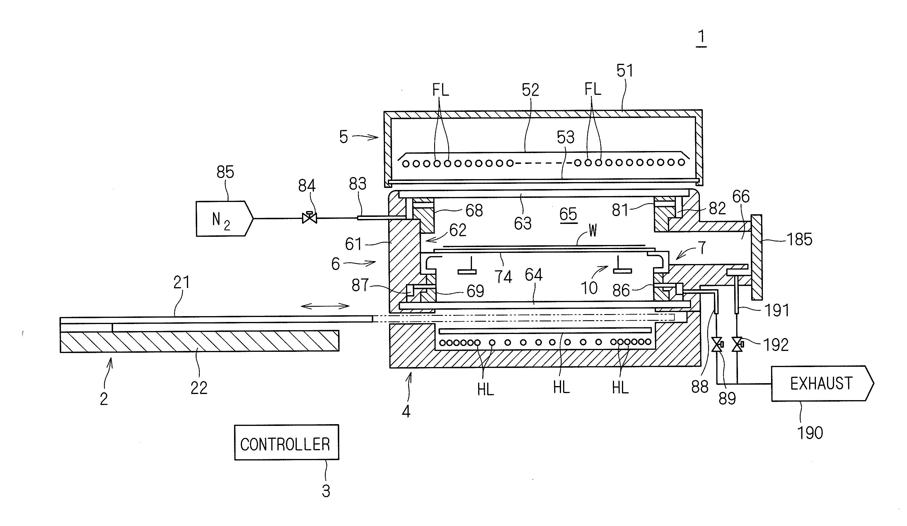
[0048]FIG. 1 is a longitudinal sectional view showing a configuration of a heat treatment apparatus 1 according to the present invention. The heat treatment apparatus 1 according to a first preferred embodiment of the present invention is a flash lamp annealer for irradiating a disk-shaped silicon semiconductor wafer W having a diameter of 300 mm and serving as a substrate with a flash of light to heat the semiconductor wafer W. A semiconductor wafer W prior to the transport into the heat treatment apparatus 1 is doped with impurities. The heat treatment apparatus 1 performs a heating treatment on the semiconductor wafer W to thereby activate the impurities introduced in the semiconductor wafer W.

[0049]The heat treatment apparatus 1 includes a chamber 6 for receiving a semiconductor wafer W therein, a flash heating part 5 including a plurality of built-in flash lamps FL, a halogen heating part 4 including a plurality of built-in halogen lamps HL, and a shutter mechanism 2. The flash...

second preferred embodiment

[0109]Next, a second preferred embodiment according to the present invention will be described. The heat treatment apparatus according to the second preferred embodiment is precisely identical in configuration with that according to the first preferred embodiment. The procedure for the treatment of a semiconductor wafer W in the heat treatment apparatus according to the second preferred embodiment is also similar to that according to the first preferred embodiment. The second preferred embodiment differs from the first preferred embodiment in the output waveform of the emission output from the flash lamp FL and, accordingly, in changes in the temperature of the semiconductor wafer W.

[0110]FIG. 15 is a graph showing changes in the temperature of the front surface of the semiconductor wafer W according to the second preferred embodiment. After the semiconductor wafer W is transported into the heat treatment space 65 and is placed on the susceptor 74, the controller 3 turns on the 40 h...


PUM


Abstract

First irradiation which causes an emission output from a flash lamp to reach its maximum value over a time period in the range of 1 to 20 milliseconds is performed to increase the temperature of a front surface of a semiconductor wafer from a preheating temperature to a target temperature for a time period in the range of 1 to 20 milliseconds. This achieves the activation of the impurities. Subsequently, second irradiation which gradually decreases the emission output from the maximum value over a time period in the range of 3 to 50 milliseconds is performed to maintain the temperature of the front surface within a ±25° C. range around the target temperature for a time period in the range of 3 to 50 milliseconds. This prevents the occurrence of process-induced damage while suppressing the diffusion of the impurities.

Description

BACKGROUND OF THE INVENTION[0001]1. Field of the Invention[0002]The present invention relates to a heat treatment method and a heat treatment apparatus for heating a thin plate-like precision electronic substrate such as a semiconductor wafer and a glass substrate for a liquid crystal display device (hereinafter referred to simply as a “substrate”) by irradiating the substrate with light, to thereby activate the impurities.[0003]2. Description of the Background Art[0004]In the process of manufacturing a semiconductor device, impurity doping is an essential step for forming a pn junction in a semiconductor wafer. At present, it is common practice to perform impurity doping by an ion implantation process and a subsequent annealing process. The ion implantation process is a technique for causing ions of impurity elements such as boron (B), arsenic (As) and phosphorus (P) to collide against the semiconductor wafer with high acceleration voltage, thereby physically implanting the impurit...

Claims


Application Information

Patent Timeline
Patent Type & Authority Applications(United States)
IPC IPC(8): H01L21/263F27B9/36
CPCH01L21/26513H01L21/2686H01L21/67115F27B17/0025H01L21/68707H01L21/68742H01L21/67248H01L21/324H01L21/02694H01L21/2253
Inventor FUSE, KAZUHIKOKATO, SHINICHIYOKOUCHI, KENICHI
Owner DAINIPPON SCREEN MTG CO LTD
Why Eureka
Try Eureka