Substrate processing method

a processing method and substrate technology, applied in the field of substrate processing method, can solve the problems of strong isotropy in etching, inability to achieve the desired shape of a hole or a trench, etc., to achieve the effect of improving processing controllability in the etching process and low energy

Inactive Publication Date: 2012-10-04
TOKYO ELECTRON LTD
View PDF7 Cites 127 Cited by
  • Summary
  • Abstract
  • Description
  • Claims
  • Application Information

AI Technical Summary

Benefits of technology

[0014]In accordance with the illustrative embodiments, a second high frequency power supply applies a high frequency voltage of a relatively low frequency to the mounting table. A DC voltage applying unit applies a DC voltage of a rectangle-shaped wave to the mounting table. If a bias voltage is generated on the mounting table by applying the high frequency voltage of the relatively low frequency to the mounting table, it is possible to obtain an ion energy distribution, formed in a certain range, having a peak of relatively low energy and a peak of relatively high energy. If the bias voltage is generated on the mounting table by...

Problems solved by technology

However, etching by ions of relatively low energy is strongly isotropic.
Also, isotropy in etching becomes strong even when anisotropy in the etching is needed.
As a result, a desired shape of a hole or ...

Method used


Image

  • Substrate processing method
  • Substrate processing method
  • Substrate processing method

Examples


Embodiment Construction

[0025]Hereinafter, illustrative embodiments will be described with reference to the accompanying drawings.

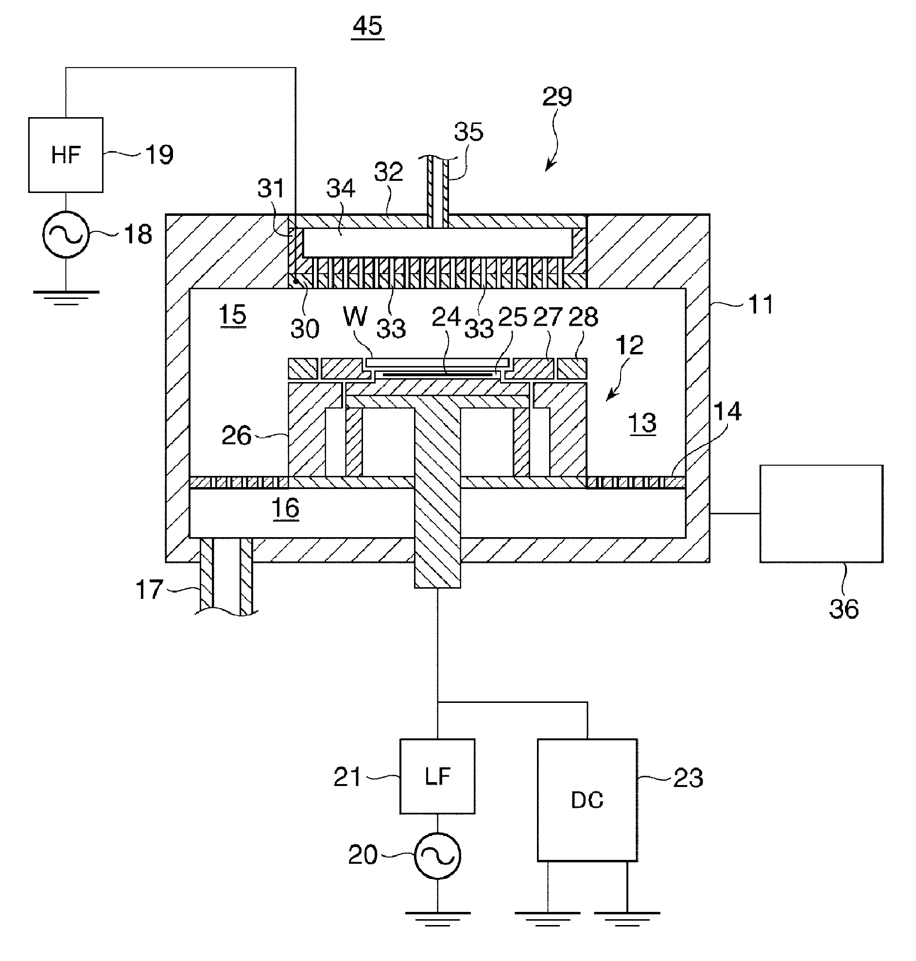
[0026]FIG. 1 is a schematic configuration view of a substrate processing apparatus in accordance with an illustrative embodiment. In the substrate processing apparatus, a plasma etching process is performed on a semiconductor device wafer (hereinafter, simply referred to as a “wafer”) as a substrate.

[0027]In FIG. 1, a substrate processing apparatus 10 includes a chamber 11 for accommodating a wafer W having a diameter of, e.g., about 300 mm, and a circular column-shaped susceptor 12 (mounting table) for mounting there on the wafer W is provided within the chamber 11. In the substrate processing apparatus 10, a side exhaust path 13 is formed between an inner sidewall of the chamber 11 and a side surface of the susceptor 12. An exhaust plate 14 is provided at a certain portion of the side exhaust path 13.

[0028]The exhaust plate 14 is a plate-shaped member having a multiple number ...


PUM

PropertyMeasurementUnit
Frequencyaaaaaaaaaa
Frequencyaaaaaaaaaa
Frequencyaaaaaaaaaa

Abstract

A substrate processing apparatus capable of improving a processing controllability in an etching process is provided. The substrate processing apparatus (10) includes a depressurized processing room (11); a susceptor (12) that is provided in the processing room (11) and configured to mount a wafer (W) thereon; a HF high frequency power supply (18) configured to apply a high frequency voltage for plasma generation to the susceptor (12); a LF high frequency power supply (20) configured to apply a high frequency voltage for a bias voltage generation to the susceptor (12); and a DC voltage applying unit (23) configured to apply a DC voltage of a rectangle-shaped wave to the susceptor (12).

Description

CROSS-REFERENCE TO RELATED APPLICATION[0001]This application claims the benefit of Japanese Patent Application No. 2011-079733 filed on Mar. 31, 2011, and U.S. Provisional Application Ser. No. 61 / 477,634 on Apr. 21, 2011, the entire disclosures of which are incorporated herein by reference.FIELD OF THE INVENTION[0002]The present disclosure relates to a substrate processing method for performing a certain process on a substrate by using plasma.BACKGROUND OF THE INVENTION[0003]A substrate processing apparatus performs a certain plasma process on a semiconductor wafer (hereinafter, referred to as simply a “wafer”) serving as a substrate by using plasma. The substrate processing apparatus includes a depressurized processing chamber; a mounting table provided in the processing chamber; a HF (High Frequency) high frequency power supply configured to be connected to the mounting table and apply a high frequency voltage of a relatively high frequency (hereinafter, referred to as a “HF high ...

Claims


Application Information

Patent Timeline
IPC IPC(8): H01L21/306H01L21/3065
CPCH01J37/32091H01J37/32706H01J37/32165H01J37/32H01J37/32082H01J37/32366H01J37/32642H01J37/32697H01J37/32724H05H1/46H01L21/3065H01J2237/327
Inventor HIMORI, SHINJIYAMADA, NORIKAZUTAKESHI, OHSE
Owner TOKYO ELECTRON LTD
Why Eureka
Try Eureka