Member for semiconductor manufacturing apparatus

a manufacturing apparatus and semiconductor technology, applied in the direction of semiconductor/solid-state device manufacturing, electric devices, basic electric elements, etc., can solve the problems of high residual stress at the time of joining and insufficient joint strength

Active Publication Date: 2012-10-04
NGK INSULATORS LTD
View PDF7 Cites 9 Cited by
  • Summary
  • Abstract
  • Description
  • Claims
  • Application Information

AI Technical Summary

Benefits of technology

[0029]According to the method for manufacturing the member for a semiconductor manufacturing apparatus according to the present invention, the above-described member for a semiconductor manufacturing apparatus according to the present invention can be produced easily. In this regard, the temperature in the heating in the step (c) may be set appropriately at a temperature, at w...

Problems solved by technology

Under such circumstances, there is a problem in that the melting point of indium is low and, therefore, in the case where the operation temperature i...

Method used


Image

  • Member for semiconductor manufacturing apparatus
  • Member for semiconductor manufacturing apparatus
  • Member for semiconductor manufacturing apparatus

Examples


examples

[0059][1] Production of Specimen

[1-1] Production Procedure of Specimen S1

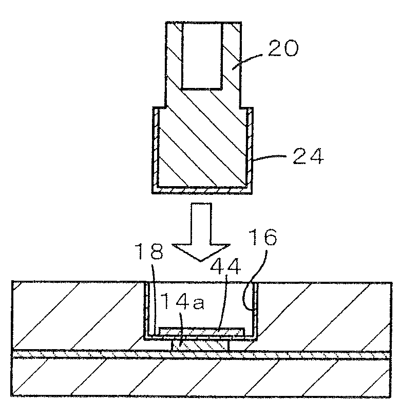
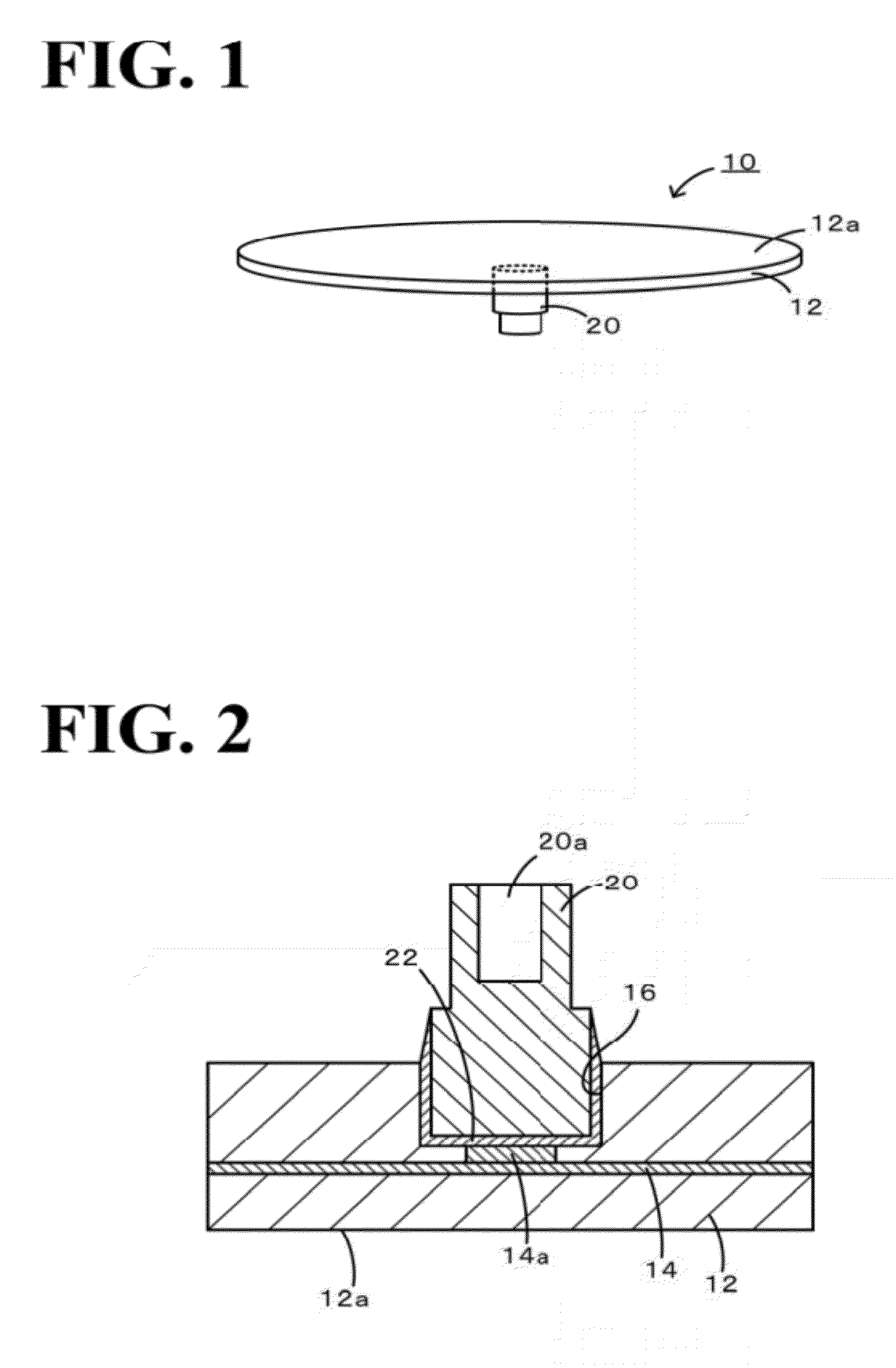
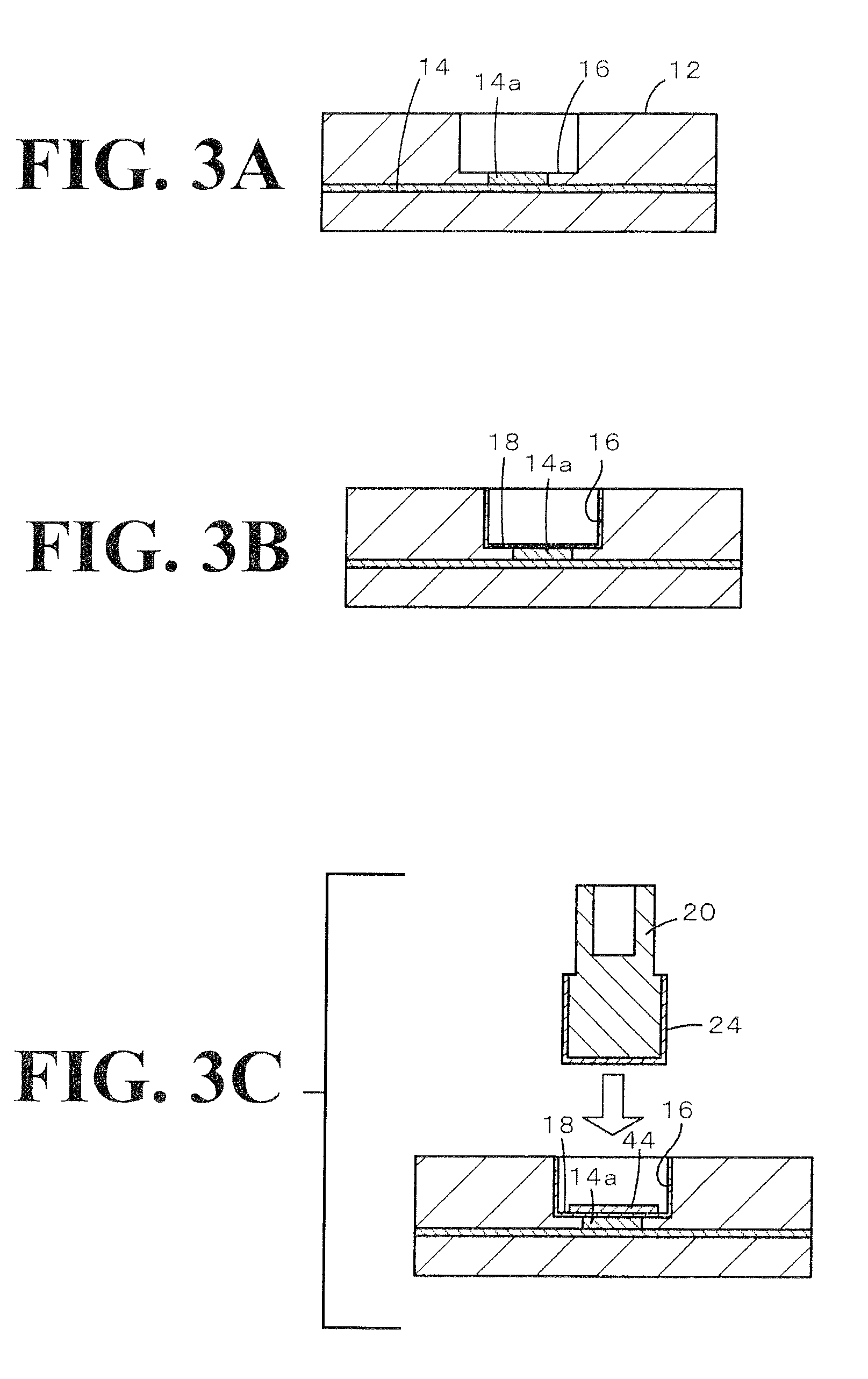
[0060]Specimen S1 simulating the joining structure shown in FIG. 2 was produced as described below. FIG. 6 is a perspective exploded view of Specimen S1. Initially, a concave portion 74 having a diameter of 6.00 mm and a depth of 0.5 mm was formed in a ceramic substrate 72 having a length of 20 mm, a width of 20 mm, and a thickness of 5 mm. Thereafter, the inside of the concave portion was subjected to a roughing treatment through sandblast, and about 3 μm of electroless Ni plating was applied. As for the material for the ceramic substrate 72, alumina (Al2O3), aluminum nitride (AlN), yttria (Y2O3), silicon carbide (SiC), and magnesia (MgO) were used. Furthermore, a power feed member 76 having a diameter of 5.95 mm and a height of 6 mm and a joining material 78 having a diameter of 5.8 mm and a foil thickness of 100 μm were prepared. Moreover, the value of the C / R ratio of a clearance C calculated by subtracting...


PUM


Abstract

An electrostatic chuck is provided with a ceramic substrate 12 in which an electrode 14 is embedded, an electrode terminal 14a exposed at the bottom of a concave portion 16 disposed on the back surface of the ceramic substrate 12, a power feed member 20 to supply an electric power to the electrode 14, and a joining layer 22 to connect this power feed member 20 to the ceramic substrate 12. The joining layer 22 is formed by using a AuGe based alloy, a AuSn based alloy, or a AuSi based alloy. The ceramic substrate 12 and the power feed member 20 are selected in such a way that the thermal expansion coefficient difference D calculated by subtracting the thermal expansion coefficient of the ceramic substrate 12 from the thermal expansion coefficient of the power feed member 20 satisfies −2.2≦D≦6 (unit: ppm/K).

Description

BACKGROUND OF THE INVENTION[0001]1. Field of the Invention[0002]The present invention relates to a member for a semiconductor manufacturing apparatus.[0003]2. Description of the Related Art[0004]In the field of semiconductor manufacturing apparatuses, alumina (Al2O3), aluminum nitride (AlN), and the like, which are dense ceramic, are used as a substrate for an electrostatic chuck. Production is performed in such a way that a high-frequency electrode is embedded in a ceramic substrate in order to generate plasma for semiconductor processing. Here, it is necessary that the electrode embedded in the ceramic substrate is electrically joined to a power feed terminal. As for this power feed terminal, a metal material having excellent electrical conductivity is used favorably. In general, the metal material has a large thermal expansion coefficient as compared with that of the ceramic. Therefore, in order to produce a product by being joined to the ceramic substrate, it is required that cr...

Claims


Application Information

Patent Timeline
IPC IPC(8): H01L21/683
CPCH01L21/6833H01L21/687
Inventor KIDA, MASAHIROHAYASE, TORUKATSUDA, YUJI
Owner NGK INSULATORS LTD
Why Eureka
Try Eureka