Step Down Current Mirror for DC/DC Boost Converters

a converter and step-down current technology, applied in the direction of dc-dc conversion, power conversion systems, instruments, etc., can solve the problems of increasing system complexity, affecting the integration of such a chip, and affecting the efficiency of dc/dc boost converters, so as to reduce the large current, reduce the cost, and reduce the cost

Inactive Publication Date: 2012-10-11
ADVANCED ANALOGIC TECHNOLOGIES INCORPORATED
View PDF3 Cites 15 Cited by
  • Summary
  • Abstract
  • Description
  • Claims
  • Application Information

AI Technical Summary

Benefits of technology

[0006]The invention eliminates the need for an off chip, low resistance, high precision resistor used to sense current in high voltage boost converters. The circuit uses a current mirror to proportionally reduce the large current that runs through the switching MOSFET of a boost converter to a smaller current. This smaller current can then be manipulated in any one of a number of ways that can be implemented within a typical lower voltage CMOS process. For example, the smaller current can be measured with a higher resistance CMOS resistor included within a typical integrated circuit. The ability to trim these high resistance resistors during the manufacturing process allows for a high degree of precision in the final DC / DC converter integrated circuit. A refinement of that embodiment would involve a second current mirror, allowing the reference resistor to be referenced to ground.

Problems solved by technology

The inclusion of this off-chip resistor as part of the DC / DC boost converter can be a significant part of the cost of the boost converter circuitry, and increases system complexity by imposing off-chip requirements on the manufacturer of the appliance rather than the more knowledgeable fabricator of the boost converter itself.
The low impedance of the resistor (in the neighborhood of 50 milliohms) makes its inclusion in such a chip problematic, as chip fabricators have difficulty fabricating a low resistance device with a high degree of required precision.
The same requirement for precision also makes the installation of Rsense into the enclosing appliance difficult, as careful traces are required in order to avoid instability in the DC / DC converter.
As a result of these factors, the cost of both the resistor itself and assembling the resistor into the final product (the television that contains the DC / DC converter, for example) is high.
Without such filtering, the noise from the MOSFET can make it difficult to accurately read (and then process) the voltage across Rsense.
With the added requirement of such filtering, there is additional cost in both the elements of the low pass filter and the careful assembly of these elements onto the circuit board of the appliance.
This becomes more problematic when it is understood that the in-circuit compensation is for an external element of the DC / DC converter circuitry, said element installed by the appliance manufacturer rather than the chip fabricator.
These additional frequency components add design complexity and design cost to the boost converter circuitry.
While it is technically possible to put S1 on the same substrate as the rest of the components, this is generally impractical because of its high voltage requirement and low resistance rating.
The inclusion of this resultantly large switch within the same substrate as the remaining boost converter components would result in a higher cost per unit that can outweigh all of the other costs outlined previously.

Method used


Image

  • Step Down Current Mirror for DC/DC Boost Converters
  • Step Down Current Mirror for DC/DC Boost Converters
  • Step Down Current Mirror for DC/DC Boost Converters

Examples


first embodiment

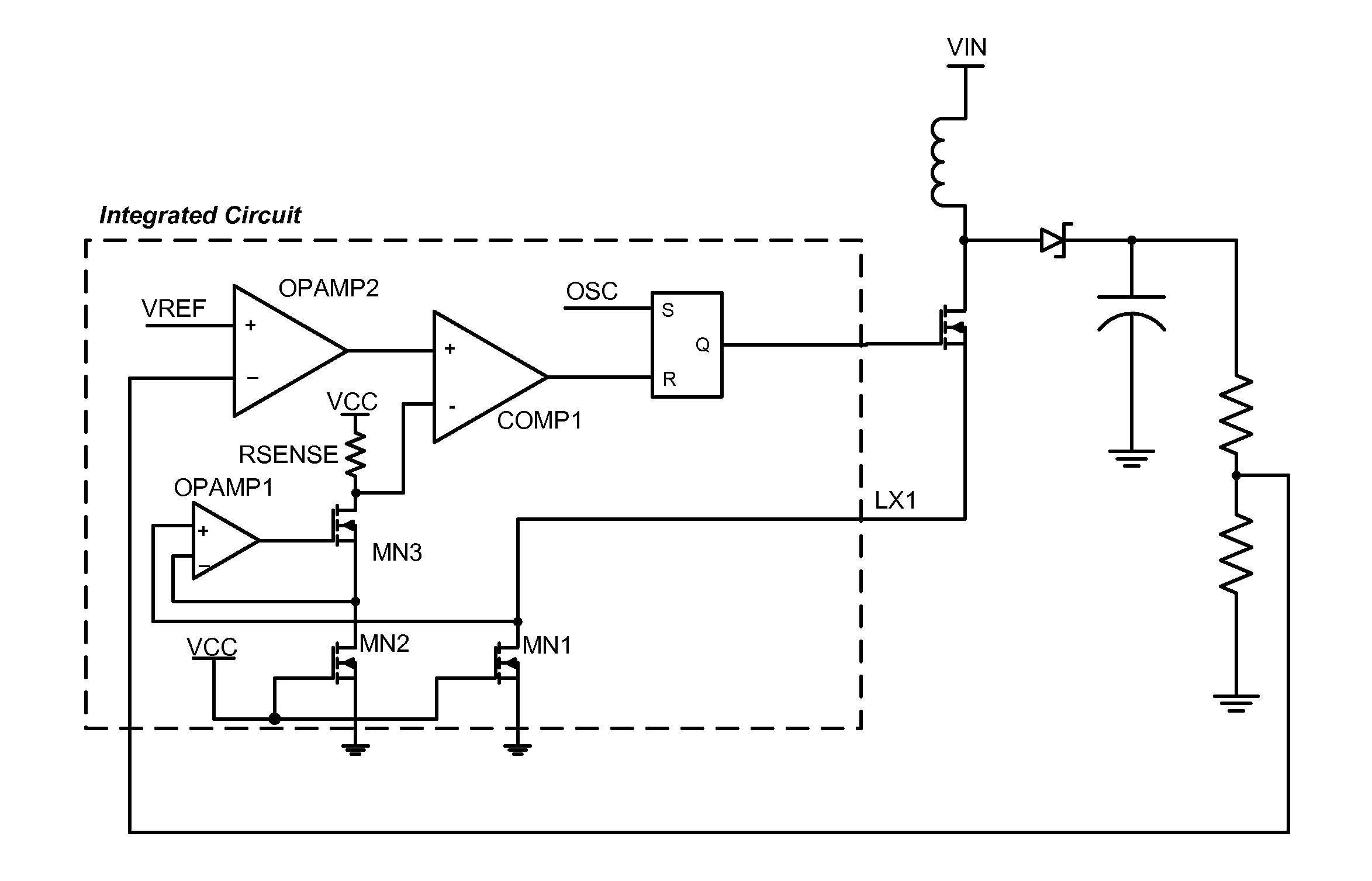
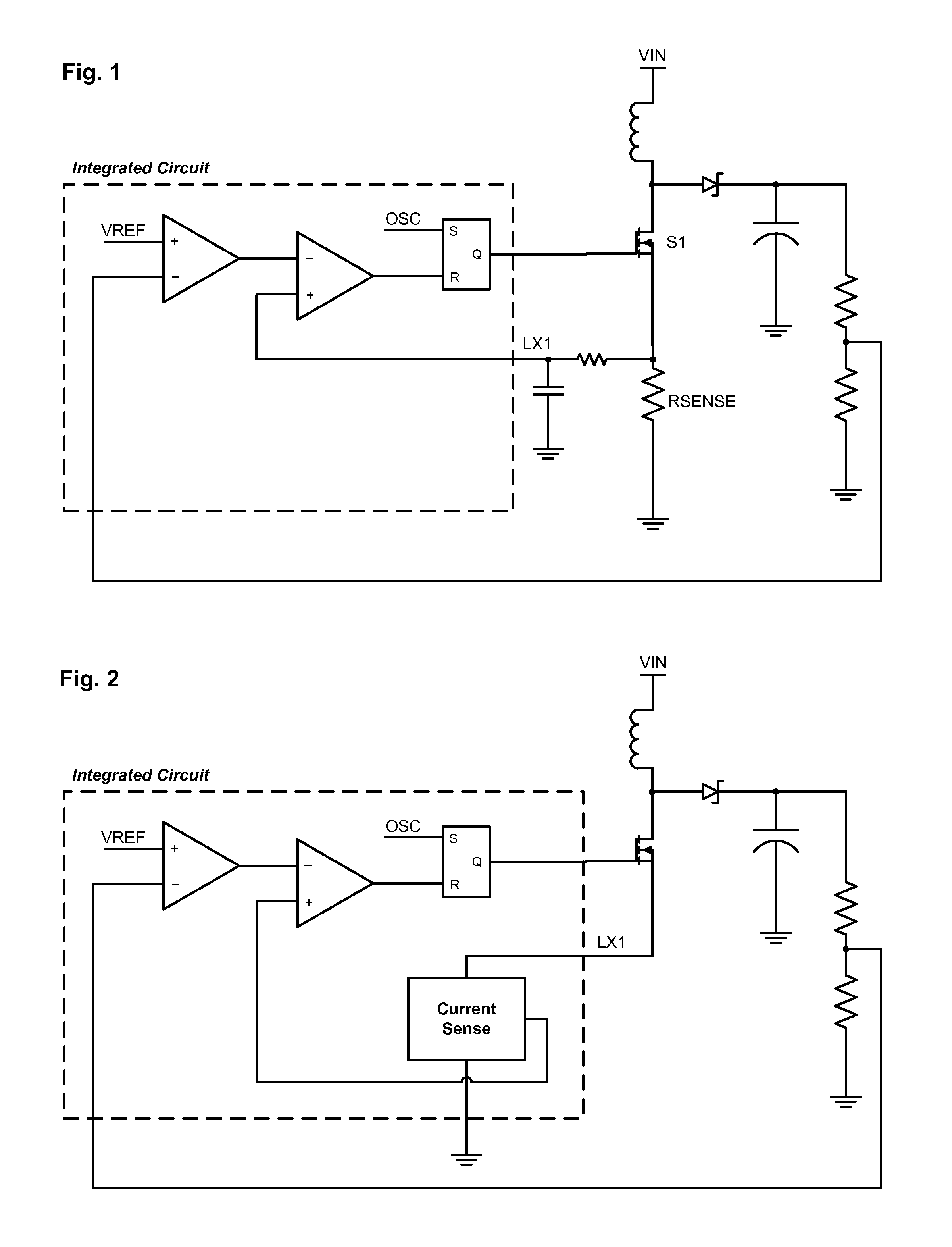
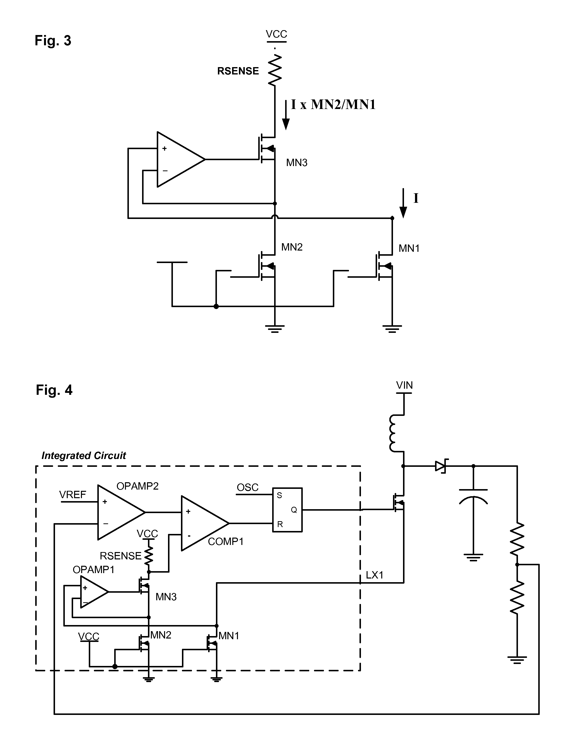
[0021]One inconvenience with this first embodiment of the invention is that the voltage across Rsense is not referenced to ground; rather, it is referenced to a voltage source. This inconvenience can be alleviated with the addition of a second current mirror, shown in FIG. 5. This simpler current mirror reflects the “first produced” current (shown as I×MN2 / MN1) into a “second produced” current that flows through a relocated Rsense resistor that is referenced to ground. Other than the difference voltage references, the two circuits function similarly.

[0022]Another embodiment of the invention utilizes directly the output current of the current mirror. Consider a boost converter in which the error element is an operational transconductance amplifier rather than the more standard operational amplifier. In this instance, the summation of the two currents—one from the OTA and the other from the current mirror—could be used directly as the input to an oscillator that drives the MOSFET. FIG...

second embodiment

[0024]FIG. 8 shows the invention as it would appear in a more complex appliance—a television with an LED backlight. In this example, the individual strings of LEDs (there could be multiple dozens of strings, or even more) are each controlled by individual current sinks. (The current sinks are controlled by a separate controller part of the television.) In order for the current sinks to function, they must have access to 1.2 volts. The black box in the drawing, which may be one IC or a series of ICs, takes as inputs the voltages above the current sinks and returns the single lowest voltage as its output, ensuring enough current for all of the strings by ensuring a minimal voltage across each of the current sinks.


PUM


Abstract

A low voltage current mirror design is used to control a high voltage boost converter. A high amperage reference current emanating from a high voltage inductor based DC-to-DC boost converter is mirrored to a low amperage output current. On-chip CMOS elements are used to measure and manipulate the output current, eliminating the need for a high precision, low resistance, external resistor. The measured and manipulated current is used to control the PWM duty cycle of an inductor based DC-to-DC boost converter, allowing for a lower cost solution in a high voltage, high current situation.

Description

BACKGROUND OF THE INVENTION[0001]One method used in modern, inductor based DC / DC boost converters to control the switching of power through the inductor utilizes a high current, low resistance, precision resistor. The resistor, shown in FIG. 1 as Rsense, is used to measure the current flowing through the inductor as the inductor is charging. The inclusion of this off-chip resistor as part of the DC / DC boost converter can be a significant part of the cost of the boost converter circuitry, and increases system complexity by imposing off-chip requirements on the manufacturer of the appliance rather than the more knowledgeable fabricator of the boost converter itself.[0002]Generally, this precision resistor is not included as part of the integrated circuit that controls the converter. The low impedance of the resistor (in the neighborhood of 50 milliohms) makes its inclusion in such a chip problematic, as chip fabricators have difficulty fabricating a low resistance device with a high d...

Claims


Application Information

Patent Timeline
Patent Type & Authority Applications(United States)
IPC IPC(8): G05F1/46
CPCG05F3/262H01L27/02H02M3/158H01L2229/00H01L2227/00G05F1/46
Inventor D'ANGELO, KEVIN
Owner ADVANCED ANALOGIC TECHNOLOGIES INCORPORATED
Why Eureka
Try Eureka