Template for Epitaxial Growth and Process for Producing Same

a technology of epitaxial growth and epitaxial growth, which is applied in the direction of crystal growth process, polycrystalline material growth, transportation and packaging, etc., can solve the problems of increasing manufacturing costs, increasing manufacturing costs, and reducing production efficiency, so as to reduce threading dislocation density and improve production efficiency , the effect of high crystal quality

Active Publication Date: 2012-10-11
NIKKISO COMPANY
View PDF3 Cites 16 Cited by
  • Summary
  • Abstract
  • Description
  • Claims
  • Application Information

AI Technical Summary

Benefits of technology

[0025]According to the method for producing a template for epitaxial growth or the template for epitaxial growth, an AlN layer or an AlGaN layer having a fine and flat surface and a reduced threading dislocation density is epitaxially grown on a sapphire (0001) substrate having recesses and protrusions on its surface by a lateral overgrowth method at a growth temperature below 1,300° C., lower than conventional growth temperature. Specifically, the initial-stage AlN layer, an underlying layer for epitaxially growing an AlN layer or an AlGaN layer thereon by a lateral overgrowth method, has portions that are epitaxially grown from the flat surface of the protrusion tops, and are oriented in the C+ axis. Specifically, the surface of the initial-stage AlN layer is an Al polar face uniformly. Thus, even at a growth temperature below 1,300° C., the AlN layer or AlGaN layer grown epitaxially from thereabove by a lateral overgrowth method has a fine and flat surface and has a reduced threading dislocation density. As a result, a GaN nitride semiconductor layer of high crystal quality is stably provided as a layer formed thereon without increasing manufacturing costs, and thus a semiconductor device having the GaN nitride semiconductor layer will have superior properties.

Problems solved by technology

Thus, the AlN underlying layer and the ELO-AlN layer cannot be grown continuously, and the manufacturing process becomes complex and the throughput decreases, thereby increasing manufacturing costs.
However, the sapphire substrate has a low etching rate and is difficult to process, so that an ELO-AlN layer having a low threading dislocation density needs to be grown on a shallow-grooved substrate.

Method used


Image

  • Template for Epitaxial Growth and Process for Producing Same
  • Template for Epitaxial Growth and Process for Producing Same
  • Template for Epitaxial Growth and Process for Producing Same

Examples


example 1 and example 2

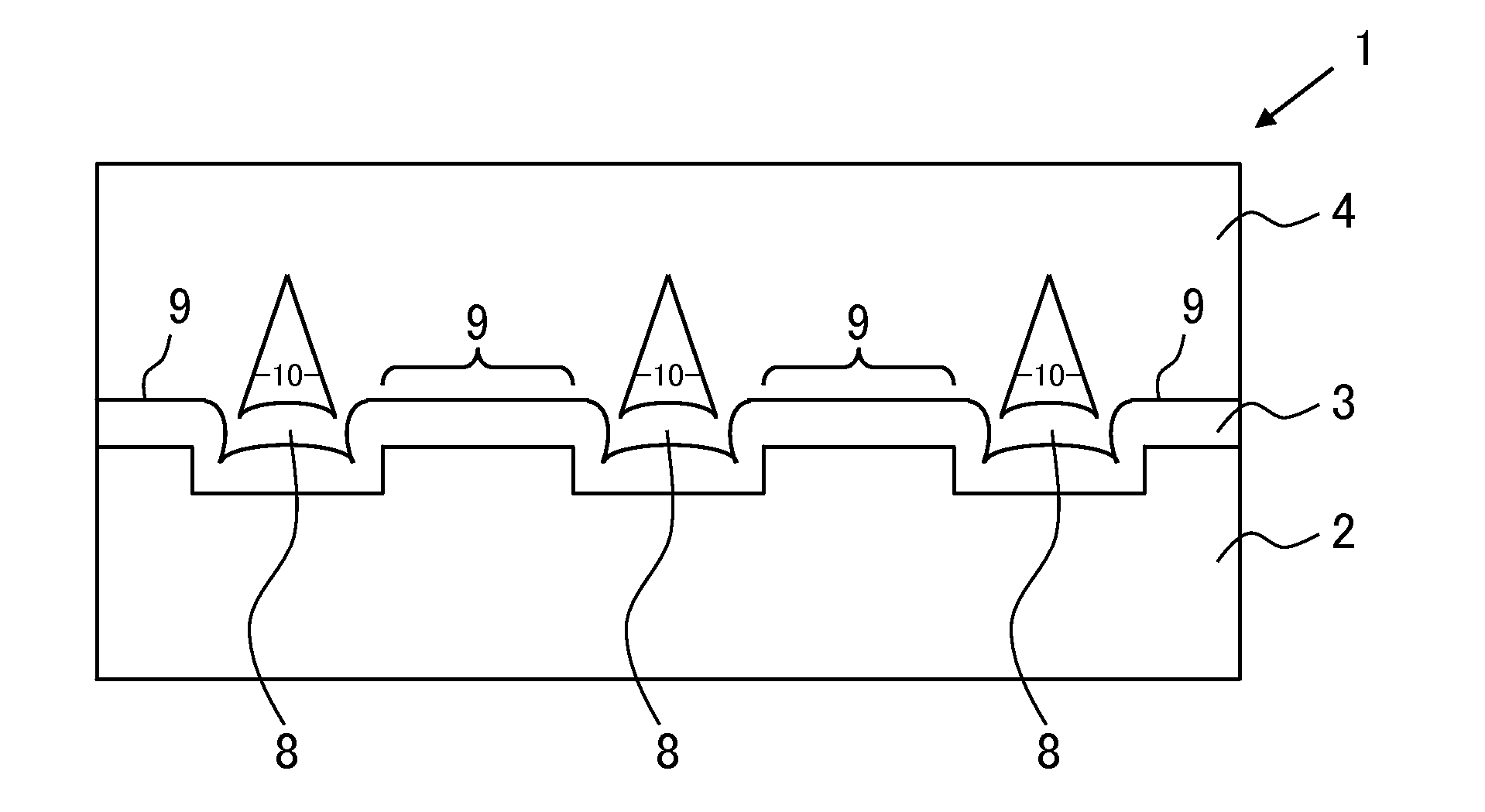
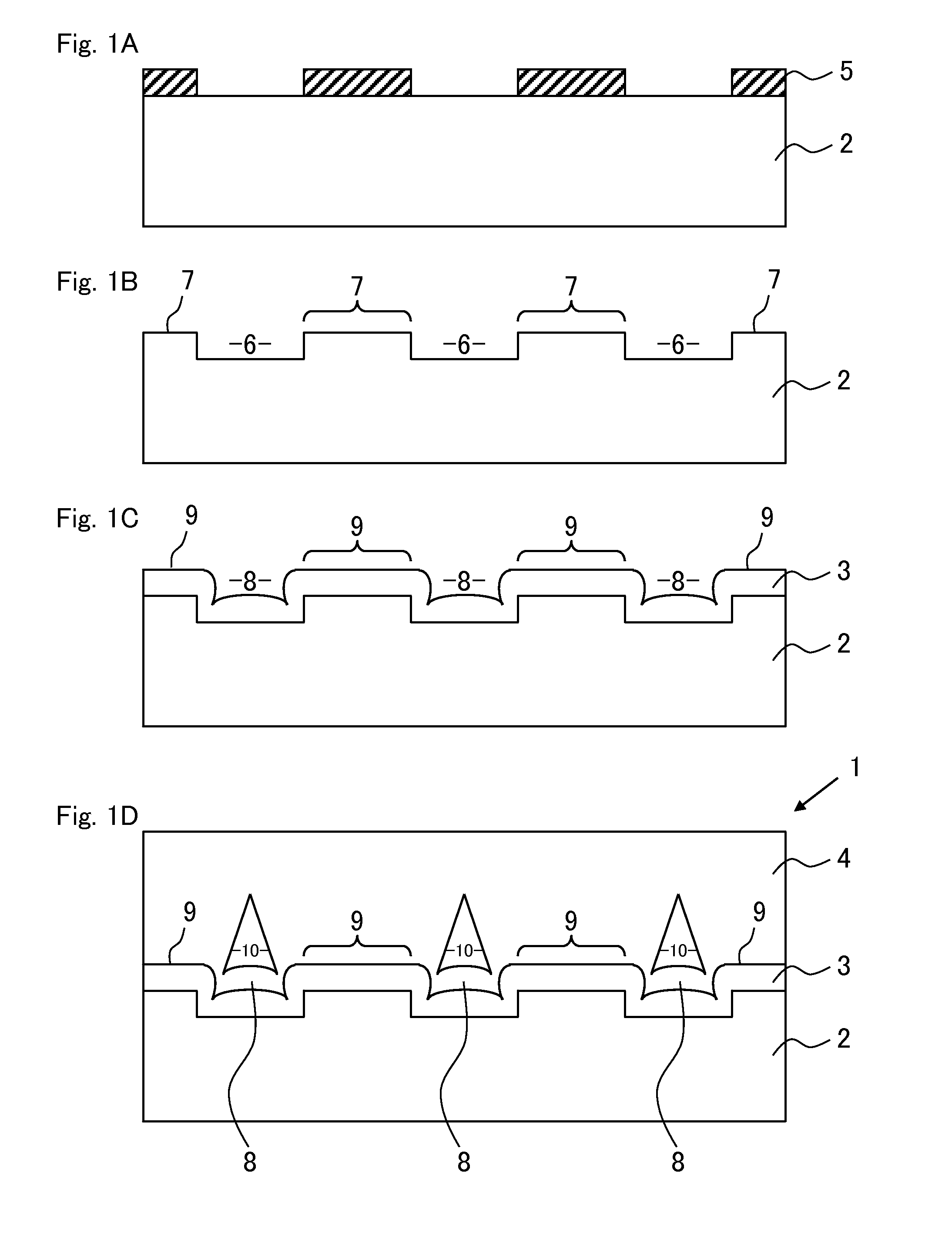
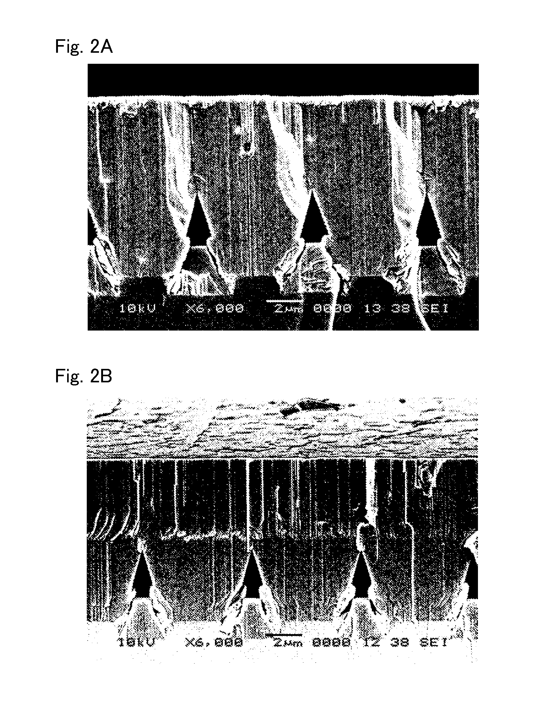
[0048]FIGS. 2A and 2B and FIGS. 3A and 3B show the SEM images (cross-sectional views 2A and 3A and bird's-eye views 2B and 3B) of Examples 1 and 2. In Example 1, the width of the grooves 6 on the surface of the sapphire substrate 2 and the gaps between the grooves 6 are 3 μm respectively, and the depth thereof is 1 μm. The thicknesses of the initial-stage AlN layer 3 and the AlN layer 4 are 1.0 μm and 9.8 μm respectively. In Example 2, the width of the grooves 6 on the surface of the sapphire substrate 2 and the gaps between the grooves 6 are 2 μm respectively, and the depth thereof is 0.5 μm. The thicknesses of the initial-stage AlN layer 3 and the AlN layer 4 are 1.0 μm and 6.2 μm respectively.

[0049]FIGS. 2A and 2B and FIGS. 3A and 3B show that the AlN layers 4 have a fine and flat surface because the layers were formed on the C+ axis oriented ininitial-stage AlN layers 3, although there is a difference in size of recesses and protrusions on the surface of the sapphire substrate 2...

example 4

[0059]FIGS. 9A and 9B show the SEM images of Example 4. FIG. 9A is a cross-sectional view and FIG. 9B is a bird's-eye view after the AlN layer 4 of Example 4 was formed and then an Al0.8Ga0.2N layer was sequentially grown thereon by the MOVPE method. The growth temperature of the Al0.8Ga0.2N layer is 1,160° C., and the flow ratio (NH3 / MO) of TMA, TMG (trimethylgallium) and NH3 is 899. In Example 5, the width of the grooves 6 formed on the surface of the sapphire substrate 2 is 5 μm; the gaps between the grooves 6 are 5 μm; and the depth thereof is 0.3 μm. The thicknesses of the initial-stage AlN layer 3, the AlN layer 4, and the Al0.8Ga0.2N layer are 1.3 μm, 5.8 μm and 1.8 μm, respectively.

[0060]FIGS. 9A and 9B clearly show that the Al0.8Ga0.2N layer formed on the AlN layer 4 also has a fine and flat surface like the AlN layer 4 by orienting the initial-stage AlN layer 3 in the C+ axis, and that the AlGaN layer of high crystal quality is formed on the present template 1. The surface...

example 5

[0061]FIG. 10 shows a cross-sectional TEM image (bright field image) after the AlN layer 4 of Example 5 was formed. In Example 5, the width of the grooves 6 on the surface of the sapphire substrate 2 and the gaps between the grooves 6 are 2 μm respectively, and the depth thereof is 0.5 μm. The thicknesses of the initial-stage AlN layer 3 and the AlN layer 4 are 1.0 μm and 6.5 μm, respectively.

[0062]FIGS. 11A and 11B show the results in which the threading dislocation density of Example 5 was evaluated, by using the cross-sectional TEM image shown in FIG. 10. In FIG. 11A, open circles ◯ indicate edge dislocation densities at three regions A to C and filled circles  indicate screw dislocation densities at three regions A to C. FIG. 11B shows average threading dislocation densities at three regions A to C. Regarding the three regions A to C, the region A indicates the region of the initial-stage AlN layer 3 above the protrusion surfaces 9 and the initial-stage growth layer of the AlN ...


PUM

PropertyMeasurementUnit
depthaaaaaaaaaa
thicknessaaaaaaaaaa
thicknessaaaaaaaaaa

Abstract

A surface of a sapphire (0001) substrate is processed to form recesses and protrusions so that protrusion tops are flat and a given plane-view pattern is provided. An initial-stage AlN layer is grown on the surface of the sapphire (0001) substrate having recesses and protrusions by performing a C+ orientation control so that a C+ oriented AlN layer is grown on flat surfaces of the protrusion tops, excluding edges, in such a thickness that the recesses are not completely filled and the openings of the recesses are not closed. An AlxGayN(0001) layer (1≧x>0, x+y=1) is epitaxially grown on the initial-stage AlN layer by a lateral overgrowth method. The recesses are covered with the AlxGayN(0001) layer laterally overgrown from above the protrusion tops. Thus, an template for epitaxial growth having a fine and flat surface and a reduced threading dislocation density is produced.

Description

CROSS-REFERENCE TO RELATED APPLICATIONS[0001]This application is a National Phase filing under 35 U.S.C. §371 of International Application No. PCT / JP2009 / 071541 filed on Dec. 25, 2009.TECHNICAL FIELD[0002]The present invention relates to a template for epitaxial growth as an underlying substrate where a GaN compound semiconductor layer (general formula: AlxGayIn1-x-yN) is epitaxially grown, and also relates to a method for producing the same.BACKGROUND ART[0003]GaN nitride semiconductor devices such as light-emitting diodes and semiconductor lasers are conventionally produced by growing a multi-layered GaN compound semiconductor layer on a template for epitaxial growth (for example, see Non-patent Document 1). FIG. 13 illustrates a typical crystal layer structure of a conventional GaN light-emitting diode. The light-emitting diode shown in FIG. 13 has a laminated structure. In the structure, after an underlying layer 102 of AlN is formed on a sapphire substrate 101 and then a cyclic...

Claims


Application Information

Patent Timeline
Patent Type & Authority Applications(United States)
IPC IPC(8): C30B25/18C30B29/40
CPCC30B25/186C30B29/403H01L21/0242H01L21/0243H01L21/02458Y10T428/24529H01L21/0262H01L21/02639H01L21/0265H01L33/007H01L21/0254H01L21/02433H01L21/02516H01L21/02609H01L21/02647H01L33/32C30B25/183C30B29/406
Inventor AMANO, HIROSHIKAMIYAMA, SATOSHIKIM, MYUNGHEEPERNOT, CYRILHIRANO, AKIRA
Owner NIKKISO COMPANY
Why Eureka
Try Eureka