Method of Forming Opening on Semiconductor Substrate

a technology of semiconductor substrate and opening, which is applied in the manufacturing of semiconductor/solid-state devices, basic electric elements, electric devices, etc., can solve the problems of line distortion on the dielectric layer, affecting the quality of products in the subsequent metallization process, etc., and achieves the effect of alleviating the phenomenon of line distortion and high etch selectivity

Active Publication Date: 2012-10-18
UNITED MICROELECTRONICS CORP
View PDF3 Cites 22 Cited by
  • Summary
  • Abstract
  • Description
  • Claims
  • Application Information

AI Technical Summary

Benefits of technology

[0010]In the present invention, a boron nitride layer is employed as the hard mask and by using different boron concentrations or by incorporating the metal nitride layer, the hard mask composite layer can include high etch selectivity with respect to the dielectric layer and the phenomenon of line distortion can be alleviated.

Problems solved by technology

When the compressive stress is directly applied to the below dielectric layer, which has low mechanical strength and tensile stress, a phenomenon of line distortion will occur on the dielectric layer.
The trenches or the vias which should be originally straight will become wiggling, therefore affecting the quality of the products in the subsequent metallization process.

Method used


Image

  • Method of Forming Opening on Semiconductor Substrate
  • Method of Forming Opening on Semiconductor Substrate
  • Method of Forming Opening on Semiconductor Substrate

Examples


Embodiment Construction

[0017]To provide a better understanding of the presented invention, preferred embodiments will be made in detail. The preferred embodiments of the present invention are illustrated in the accompanying drawings with numbered elements.

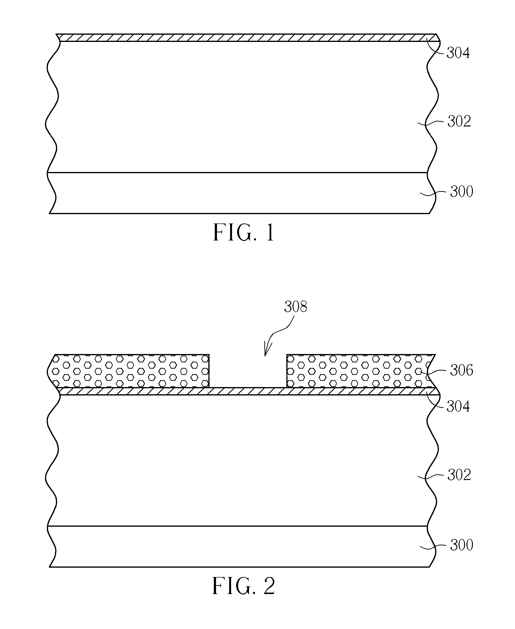
[0018]Please refer to FIG. 1 to FIG. 3, illustrating schematic diagrams of the method of forming an opening on the semiconductor substrate according to the first embodiment in the present invention. As shown in FIG. 1, firstly, a substrate 300 is provided. The substrate 300, for example, includes a silicon substrate, an epitaxial silicon substrate, a silicon germanium substrates, a silicon-on-insulator (SOI) substrate, a glass substrate, a quartz substrate, or a ceramic substrate, but should not be limited thereto. Besides, at least a conductive component (not shown) can be disposed on the substrate 300. The conductive component can be the source / drain region of CMOS, the through-silicon via (TSV), the doped region or the metal interconnection layers. De...


PUM

PropertyMeasurementUnit
dielectric constantaaaaaaaaaa
thicknessaaaaaaaaaa
semiconductoraaaaaaaaaa

Abstract

The present invention provides a method of forming an opening on a semiconductor substrate. First, a substrate is provided. Then a dielectric layer and a cap layer are formed on the substrate. A ratio of a thickness of the dielectric layer and a thickness of the cap layer is substantially between 15 and 1.5. Next, a patterned boron nitride layer is formed on the cap layer. Lastly, an etching process is performed by using the patterned hard mask as a mask to etch the cap layer and the dielectric layer so as to form an opening in the cap layer and the dielectric layer.

Description

BACKGROUND OF THE INVENTION[0001]1. Field of the Invention[0002]The present invention relates to a method of forming an opening on a semiconductor substrate, and especially to a method of forming an opening by using boron nitride as a hard mask such that the phenomenon of line distortion in conventional damascene processes can be prevented.[0003]2. Description of the Prior Art[0004]Damascene interconnect processes incorporated with copper are known in the art, which are also referred to as “copper damascene processes” in the semiconductor industry. Generally, the copper damascene processes are categorized into single damascene process and dual damascene process. Because the dual damascene has advantages of simplified processes, lower contact resistance between wires and plugs, and improved reliance, it is widely applied in a damascene interconnect technique. In addition, for reducing resistance and parasitic capacitance of the multi-level interconnect and improving speed of signal t...

Claims


Application Information

Patent Timeline
Patent Type & Authority Applications(United States)
IPC IPC(8): H01L21/311
CPCH01L21/76802H01L21/31144
Inventor WU, CHUN-YUANLIU, CHIH-CHIENLIN, CHIN-FUCHEN, PO-CHUN
Owner UNITED MICROELECTRONICS CORP
Why Eureka
Try Eureka