Nanostructures, Systems, and Methods for Photocatalysis

a photocatalysis and nanostructure technology, applied in the field of nanostructures and, can solve the problems of low efficiency of systems, light not readily causing each of these chemical reactions to occur,

Active Publication Date: 2012-10-25
PRESIDENT & FELLOWS OF HARVARD COLLEGE
View PDF14 Cites 91 Cited by
  • Summary
  • Abstract
  • Description
  • Claims
  • Application Information

AI Technical Summary

Problems solved by technology

However, light does not readily cause each of these chemical reactions to occur and catalysts are needed to effect the overall transformation with efficiencies suitable for practical applications.
Traditional approaches to photocatalysis have relied on the use of expensive materials and / or systems that operate with low efficiency.

Method used


Image

  • Nanostructures, Systems, and Methods for Photocatalysis
  • Nanostructures, Systems, and Methods for Photocatalysis
  • Nanostructures, Systems, and Methods for Photocatalysis

Examples


example 1

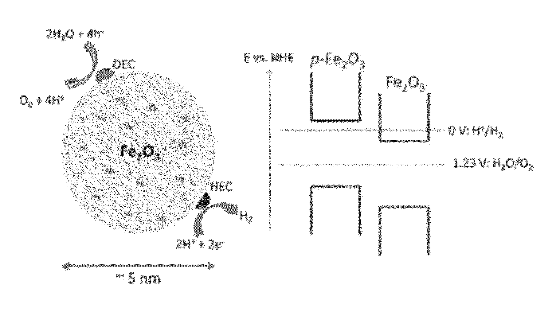
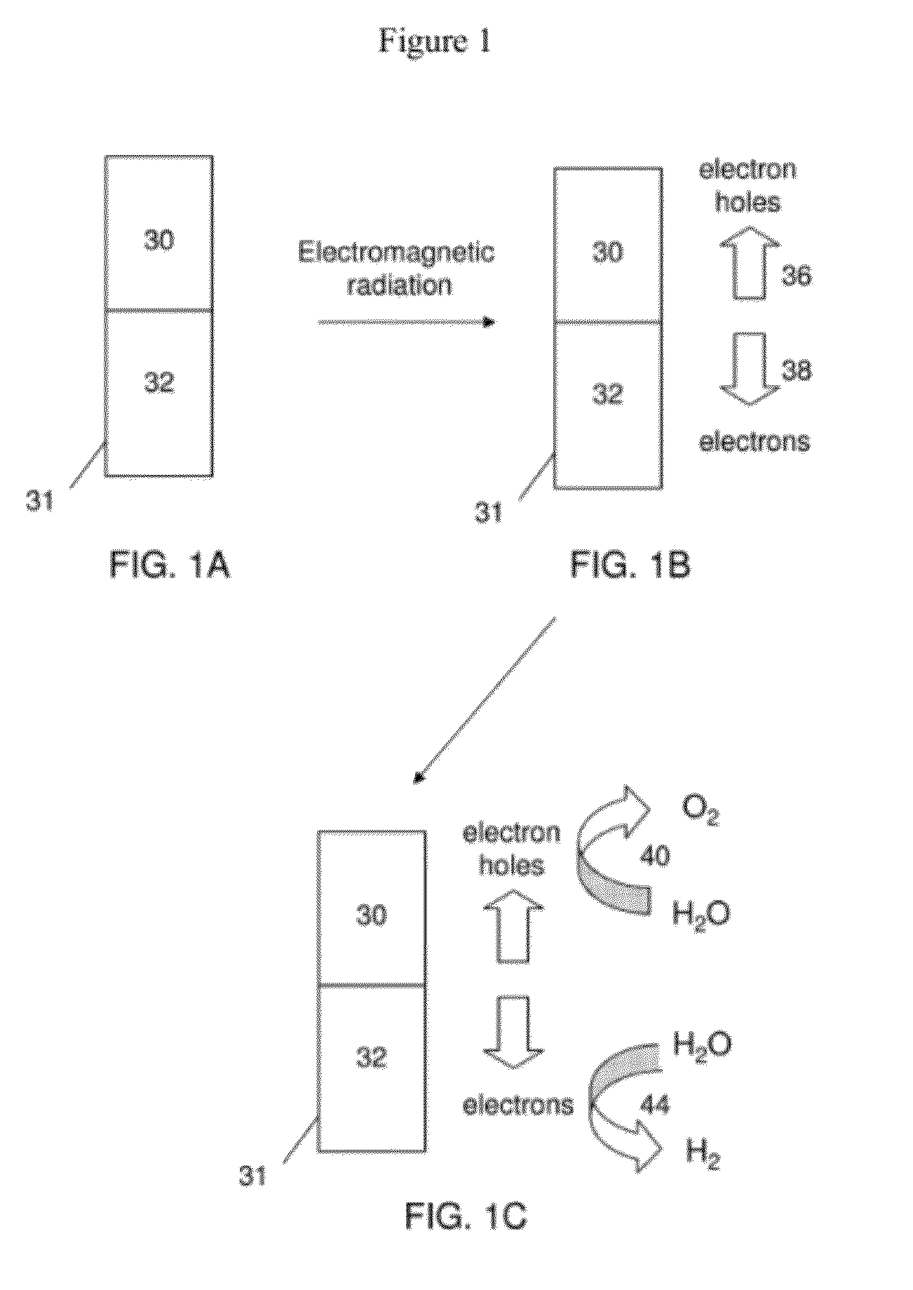
[0251]The following prophetic example describes photocatalytic production of hydrogen and oxygen gases from water using a colloidal suspension of p / n-doped nanowires or nanorods. The nanowires are comprised of at least one semiconductor material, such that a p / n-junction is formed within the nanowires or nanorods. Upon exposure to electromagnetic radiation, excited electrons travel to one end of the nanowires or nanorod and the corresponding electron hole travels to the other end.

[0252]In this example, an iron oxide employed as the semiconductor. Iron oxide semiconductor material is generally stable to corrosion under the conditions for water splitting. In addition, the band positions and band gap of a p / n-junction of an iron oxide is appropriate for (1) efficient absorption of visible light, and (2) the production of hydrogen and oxygen gas from water (e.g., see Leygraf et al., J. Catalysis 1982, 78, 341-351; Turner et al., J. Electrochem Soc. 1984, 131, 1777-1783). The p-type and ...

example 2

[0255]The following prophetic example describes photocatalytic production of hydrogen and oxygen gases from water using a colloidal suspension of dye-sensitized nanoparticles. Most of the photocatalyst materials explored to date are comprised of metal oxide semiconductors having bandgaps of 3 eV or larger. These materials have proven to be excellent photocatalysts for water oxidation, however their poor absorption of visible light limits the overall efficiency for solar energy conversion. Photoactive dye molecules may be chemically adsorbed to the surface of wide bandgap, metal oxide particles that have been loaded with catalysts for the hydrogen evolution reaction (HER). In this scheme, excitation of the dye molecule promotes the transfer of an electron from the dye to the particle. The electron resides in the semiconductor conduction band, allowing transport of the electron to the hydrogen evolution catalyst. The corresponding electron hole remains on the dye, where it is later co...


PUM

PropertyMeasurementUnit
diametersaaaaaaaaaa
transmittanceaaaaaaaaaa

Abstract

The present invention generally relates to nanostructures and compositions comprising nanostructures, methods of making and using the nanostructures, and related systems. In some embodiments, a nanostructure comprises a first region and a second region, wherein a first photocatalytic reaction (e.g., an oxidation reaction) can be carried out at the first region and a second photocatalytic reaction (e.g., a reduction reaction) can be carried out at the second region. In some cases, the first photocatalytic reaction is the formation of oxygen gas from water and the second photocatalytic reaction is the formation of hydrogen gas from water. In some embodiments, a nanostructure comprises at least one semiconductor material, and, in some cases, at least one catalytic material and / or at least one photosensitizing agent.

Description

RELATED APPLICATIONS[0001]This application claims priority to U.S. application 61 / 478,364, “Nanostructures, Systems, and Methods for Photocatalysis,” filed Apr. 22, 2011; to U.S. application 61 / 566,078, “Systems and Methods for Photocatalytic Production of Hydrogen from Water,” filed Dec. 2, 2011; and to U.S. application 61 / 581,822, “Materials for Photocatalytic Splitting of Water into Hydrogen and Oxygen, filed Dec. 30, 2011.” All of the foregoing applications are incorporated herein by reference in their entireties for any and all purposes.STATEMENT OF GOVERNMENT INTEREST[0002]This invention was made with the support under government contract DE-AR0000036, awarded by the Department of Energy (DOE) Advanced Research Project Agency-Energy (ARPA-E). The government has certain rights in the invention.FIELD OF THE INVENTION[0003]The present invention relates to the field of nanostructures and to the field of photocatalytic reactions.BACKGROUND OF THE INVENTION[0004]Photocatalysis invol...

Claims


Application Information

Patent Timeline
Patent Type & Authority Applications(United States)
IPC IPC(8): H01B1/00C01B13/02B01J37/34B01J19/12B82Y30/00B82Y40/00
CPCB01J19/127B01J19/2475B01J23/745B01J35/0013B01J35/004C25B1/003B82Y30/00C01B3/042C01B13/0207Y02E60/364Y02E60/368B01J35/06C25B1/55Y02E60/36Y02P20/133
Inventor REECE, STEVEN Y.JARVI, THOMAS D.
Owner PRESIDENT & FELLOWS OF HARVARD COLLEGE
Why Eureka
Try Eureka