Thin film transistor and fabrication method thereof

a technology of thin film transistors and fabrication methods, which is applied in the direction of transistors, semiconductor devices, electrical equipment, etc., can solve the problems of discontinuous formation of pixel electrodes on the passivation layer, and achieve the effect of favorable stability

Active Publication Date: 2012-10-25
AU OPTRONICS CORP
View PDF3 Cites 13 Cited by
  • Summary
  • Abstract
  • Description
  • Claims
  • Application Information

AI Technical Summary

Benefits of technology

[0007]The invention is directed to a thin film transistor having favorable stability.

Problems solved by technology

Moreover, during the etching process, an etching undercut may occur in the passivation layer and the underlying gate insulating layer, causing the discontinuous formation of the pixel electrode on the passivation layer.

Method used


Image

  • Thin film transistor and fabrication method thereof
  • Thin film transistor and fabrication method thereof
  • Thin film transistor and fabrication method thereof

Examples


first embodiment

The First Embodiment

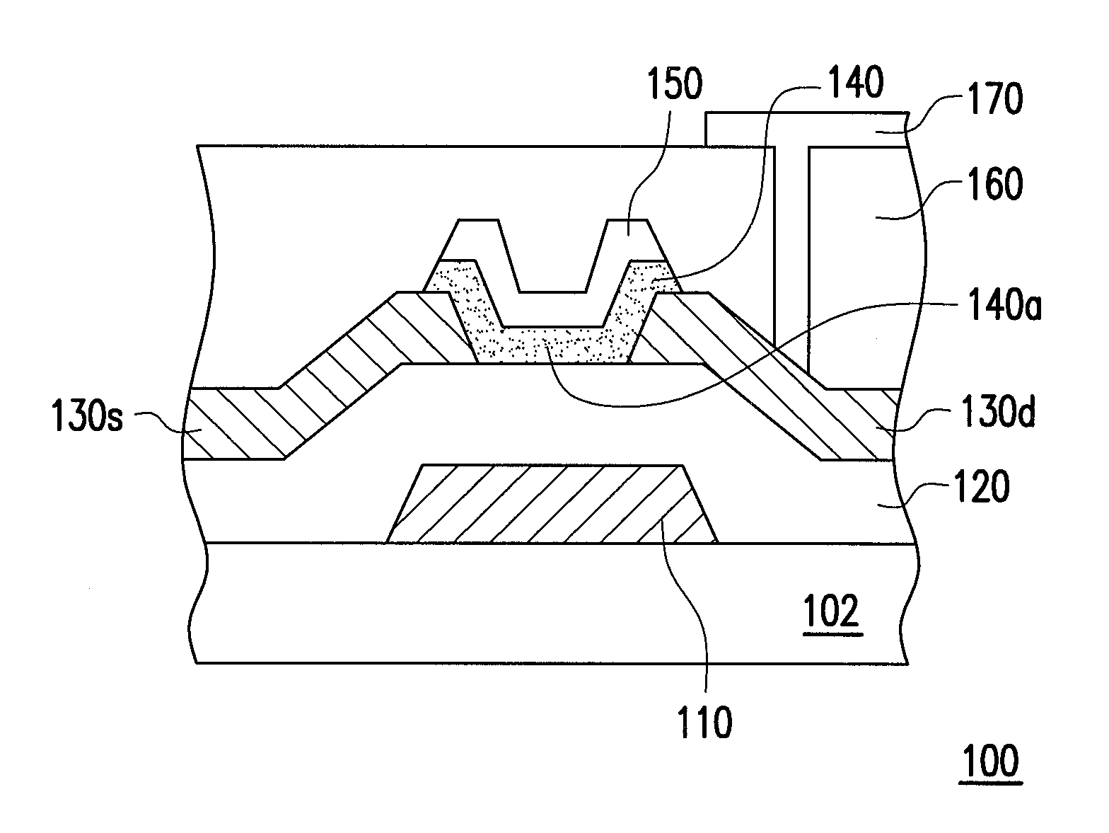
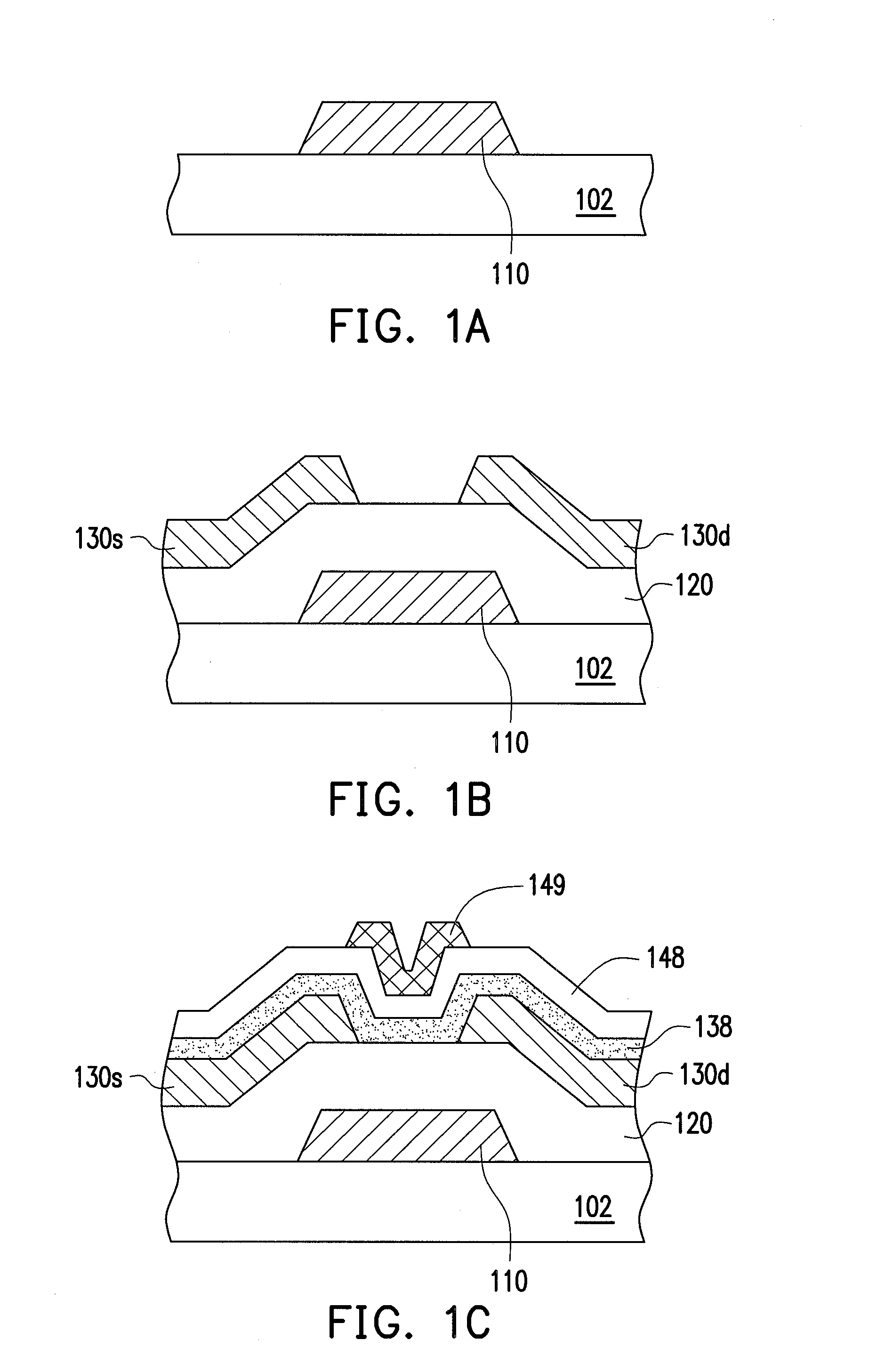
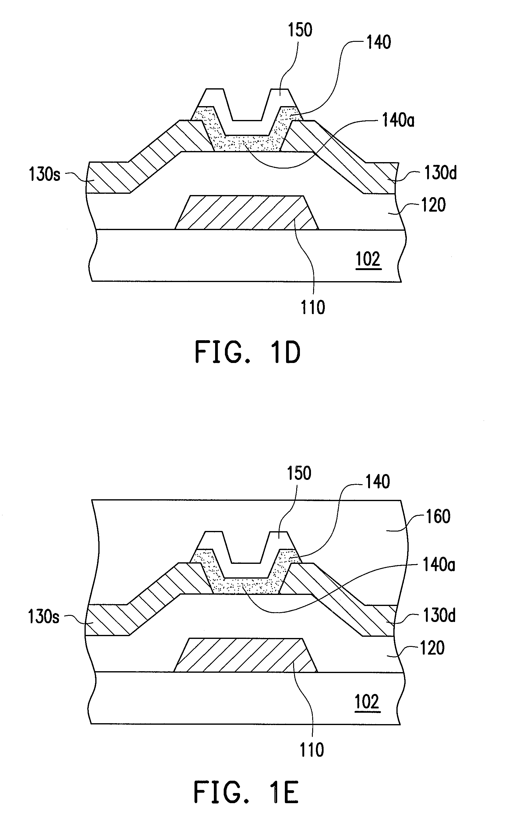
[0017]FIG. 1A to FIG. 1F are schematic cross-sectional views showing a fabrication method of a thin film transistor according to the first embodiment of the invention. Reference with FIG. 1A, first, a gate 110 is formed on a substrate 102. In this embodiment, the substrate 102 can be a glass substrate or other suitable substrate, which is not limited in the invention. The gate 110 may have a single-layer or multiple-layer structure of the conductive material, and the conductive material can be selected from the group consisting of copper (Cu), molybdenum (Mo), titanium (Ti), aluminum (Al), tungsten (W), silver (Ag), gold (Au), and an alloy thereof. A method of forming the gate 110 is patterning a conductive layer by photolithography and etching processes, for example. In this embodiment, the gate 110 has, for example, a stacked structure of titanium / aluminum / titanium.

[0018]Reference with FIG. 1B, then, a gate insulating layer 120 is formed on the gate 110. The ga...

second embodiment

The Second Embodiment

[0027]FIG. 2A to FIG. 2F are schematic cross-sectional views showing a fabrication method of a thin film transistor according to a second embodiment of the invention. With reference to FIG. 2A, first, a gate 110 is formed on a substrate 102. According to the present embodiment, materials of the substrate 102 and the gate 110 are similar to those provided in the first embodiment, and thus further descriptions are omitted.

[0028]Reference with FIG. 2B, then, a gate insulating layer 120 is formed on the gate 110. The gate insulating layer 120 may have a single-layer or multiple-layer structure, and a material thereof may be dielectric material such as silicon oxide, silicon nitride or silicon oxynitride.

[0029]Next, a channel layer 140 is formed on the gate insulating layer 120. A material of the channel layer 140 includes IGZO, and a method of forming the channel layer 140 includes PVD, for example.

[0030]Reference with FIG. 2C, a source 130s and a drain 130d are for...

experimental example

[0037]In order to verify that the thin film transistor according to the above embodiments has better device characteristics, an experimental example is compared with a comparative example. The thin film transistor according to the experimental example has a structure as shown in FIG. 1F, wherein the material of the first patterned passivation layer is aluminum oxide, the thickness of the first patterned passivation layer is 10 nm, the material of the second patterned passivation layer is acrylic polymer, and the thickness of the second patterned passivation layer is 1.5 um. The thin film transistor according to the comparative example has a structure similar to the thin film transistor according to the experimental example, except that the thin film transistor according to the comparative example doesn't have the second patterned passivation layer. In other words, the thin film transistor according to the comparative example only has the first patterned passivation layer, wherein th...


PUM


Abstract

A thin film transistor is provided. The thin film transistor includes a substrate, a gate, a gate insulating layer, a source and a drain, a channel layer, and first and second patterned passivation layers. The gate is disposed on the substrate. The gate insulating layer is disposed on the gate. The source and the drain are disposed on the gate insulating layer. The channel layer is disposed above or under the source and the drain, wherein a portion of the channel layer is exposed between the source and the drain. The first patterned passivation layer is disposed on the portion of the channel layer, wherein the first patterned passivation layer includes metal oxide, and the first patterned passivation layer has a thickness ranging from 50 angstroms to 300 angstroms. The second patterned passivation layer covers the first patterned passivation layer, the gate insulating layer, and the source and the drain.

Description

CROSS-REFERENCE TO RELATED APPLICATION[0001]This application claims the priority benefit of Taiwan application serial no. 100114110, filed Apr. 22, 2011. The entirety of the above-mentioned patent application is hereby incorporated by reference herein and made a part of this specification.BACKGROUND OF THE INVENTION[0002]1. Field of the Invention[0003]The invention relates to a semiconductor device and a fabrication method thereof, and more particularly to a thin film transistor and a fabrication method thereof.[0004]2. Description of Related Art[0005]In general, a liquid crystal display (LCD) mainly includes a thin film transistor (TFT) array substrate, a color filter substrate, and a liquid crystal layer sandwiched between the two substrates. An amorphous silicon TFT or a low temperature polysilicon TFT is usually adopted as a switch device of each sub-pixel in the TFT array substrate. In recent years, it is reported that, the oxide semiconductor TFT has relatively high carrier mo...

Claims


Application Information

Patent Timeline
Patent Type & Authority Applications(United States)
IPC IPC(8): H01L29/786H01L21/336
CPCH01L29/7869H01L29/4908
Inventor CHEN, CHIA-HSIANGHUNG, MING-CHINTU, CHUN-HAOLIN, WEI-TINGCHANG, JIUN-JYE
Owner AU OPTRONICS CORP
Why Eureka
Try Eureka