Semiconductor device

a technology of semiconductors and transistors, applied in the direction of semiconductor devices, basic electric elements, electrical appliances, etc., can solve the problems of short-channel effect and other problems, and achieve the effect of preventing defects, and reducing the size of transistors

Inactive Publication Date: 2012-10-25
SEMICON ENERGY LAB CO LTD
View PDF5 Cites 20 Cited by
  • Summary
  • Abstract
  • Description
  • Claims
  • Application Information

AI Technical Summary

Benefits of technology

[0021]According to one embodiment of the disclosed invention, a method for manufacturing a semiconductor device which prevents a defect and achieves miniaturization can be provided.
[0022]In addition, according to one embodiment of the disclosed invention, the size of a transistor can be sufficiently reduced. When the size of the transistor is sufficiently reduced, the size of a semiconductor device is also reduced and thus the number of semiconductor devices manufactured from o...

Problems solved by technology

In the case where a transistor is miniaturized...

Method used


Image

  • Semiconductor device
  • Semiconductor device
  • Semiconductor device

Examples


embodiment 1

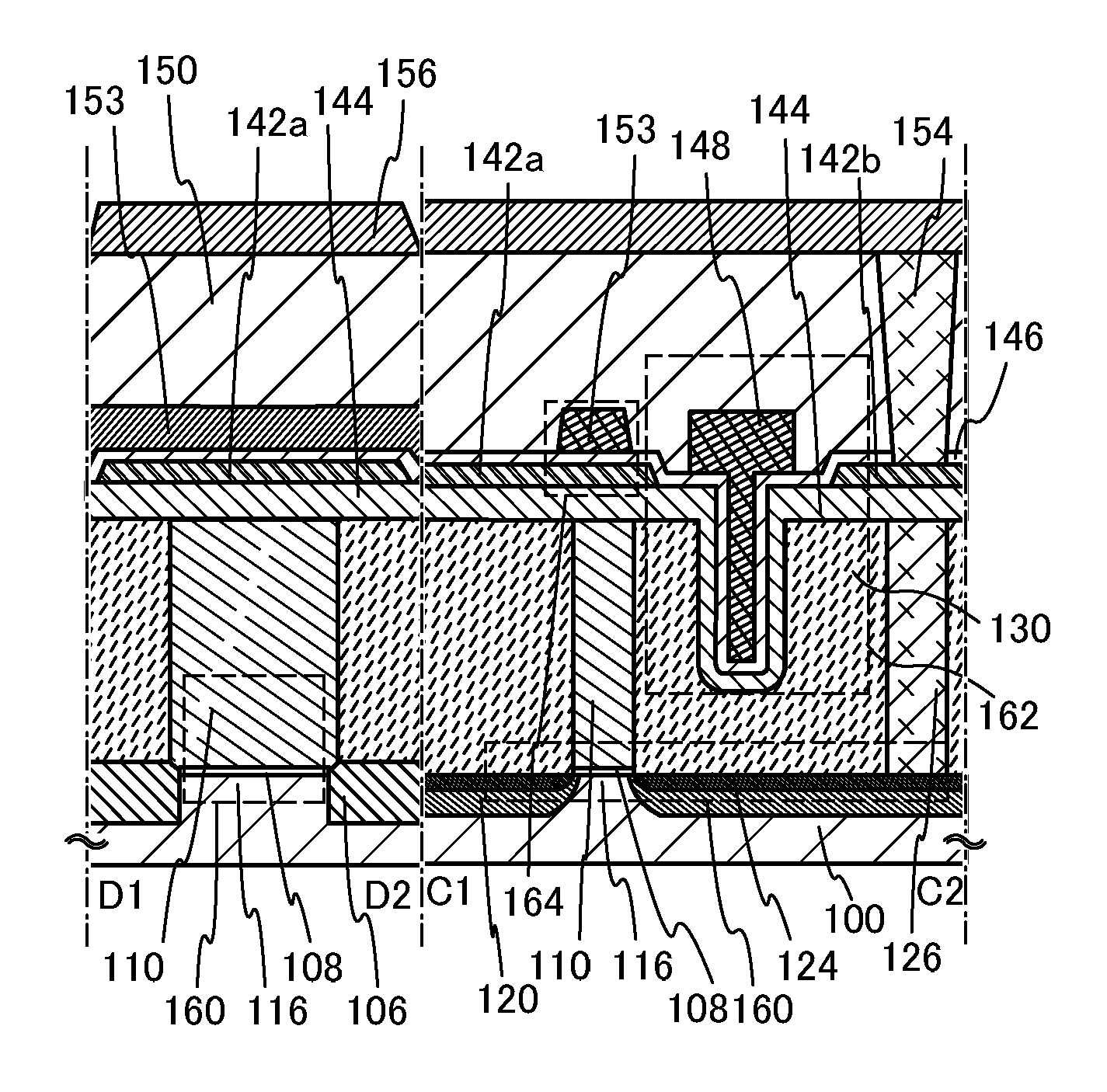
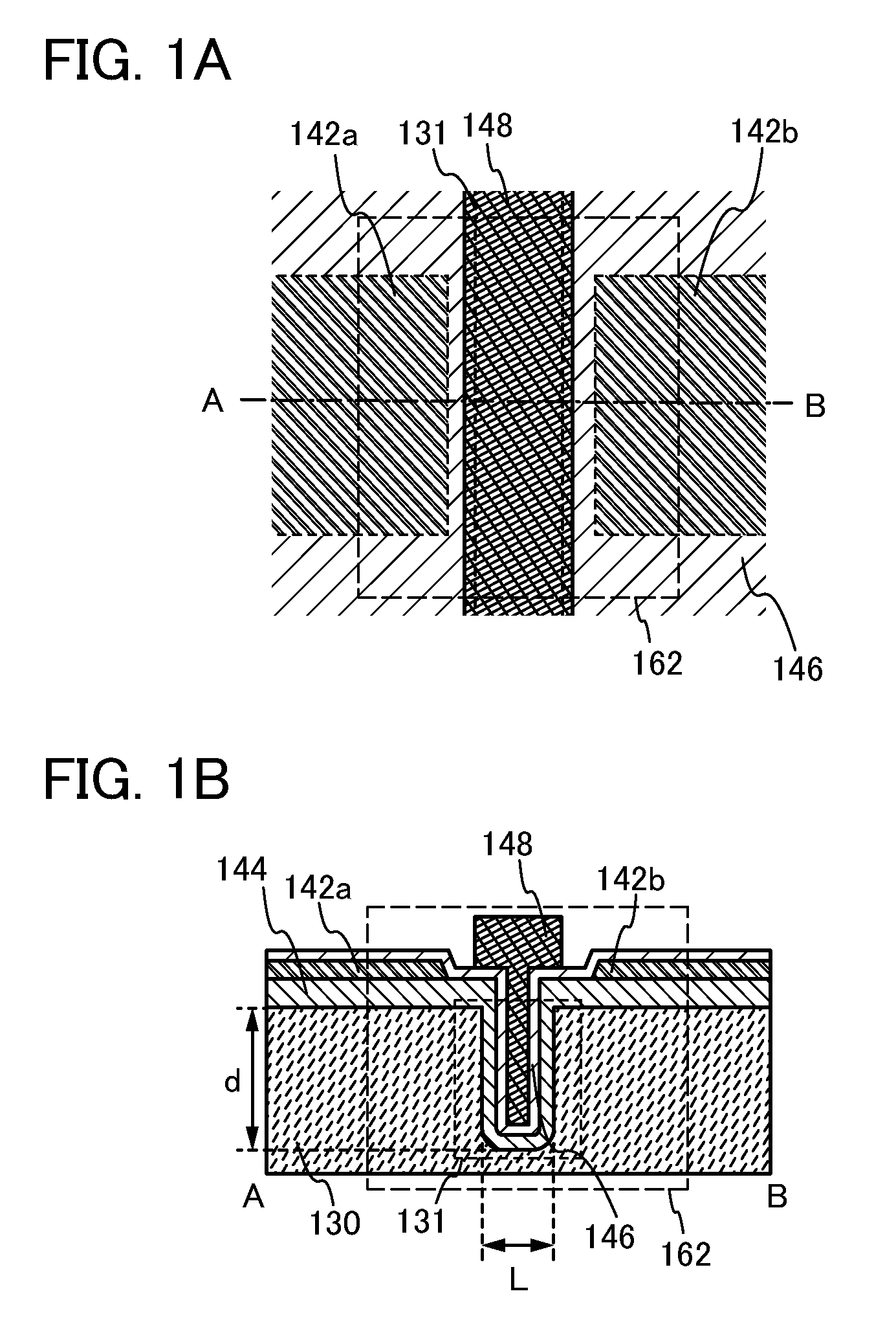
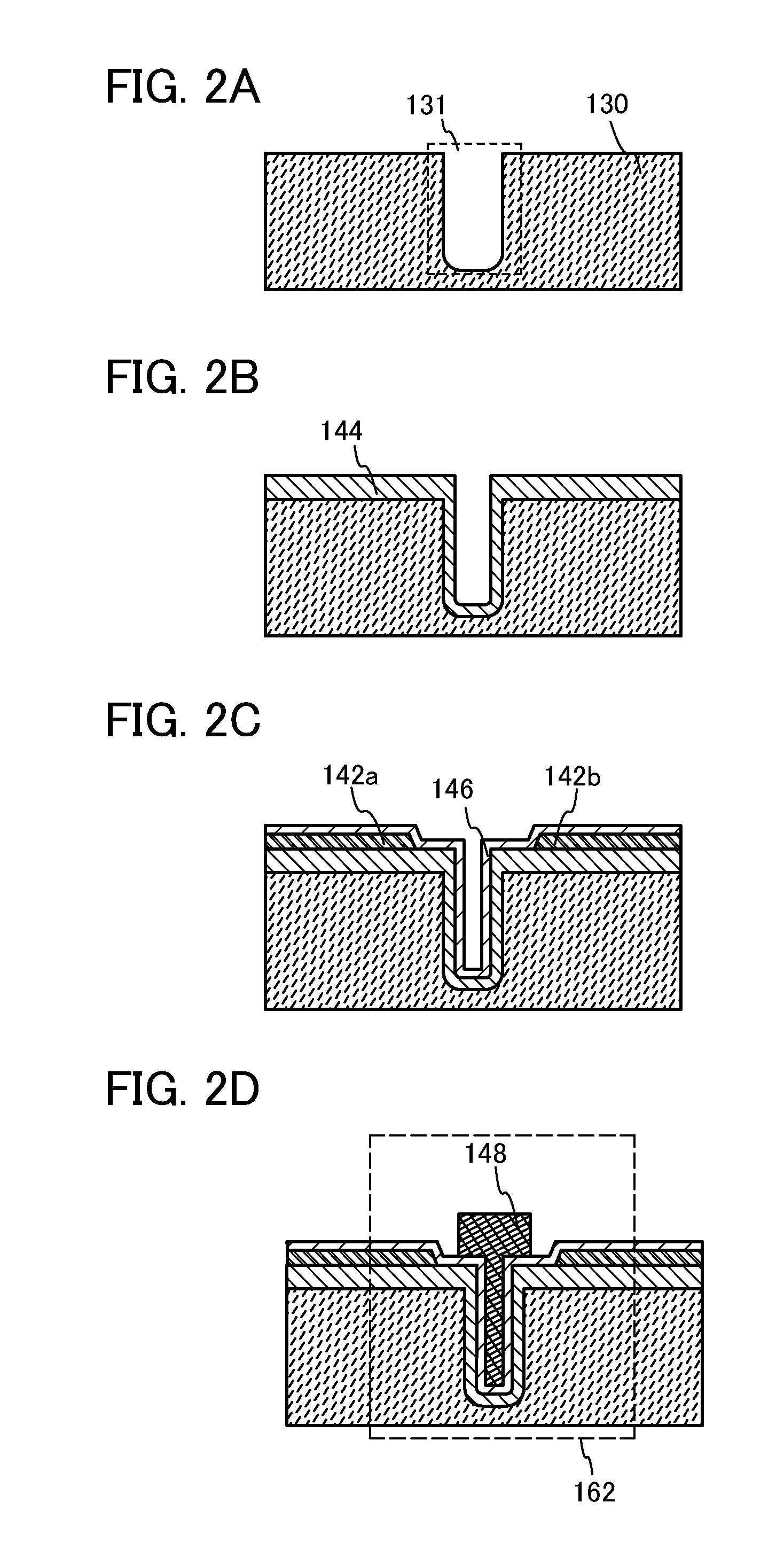
[0037]In this embodiment, an example of a semiconductor device and a manufacturing process thereof according to one embodiment of the disclosed invention will be described with reference to FIGS. 1A and 1B.

[0038]In this embodiment, an example in which an oxide semiconductor is used as a wide-gap semiconductor which can be applied to a transistor is described. As an oxide semiconductor, an oxide semiconductor having a band gap larger than at least 1.1 eV, which is the band gap of silicon, can be applied; for example, an In—Ga—Zn—O-based oxide semiconductor having a band gap of 3.15 eV, indium oxide having a band gap of about 3.0 eV, indium tin oxide having a band gap of about 3.0 eV, indium gallium oxide having a band gap of about 3.3 eV, indium zinc oxide having a band gap of about 2.7 eV, tin oxide having a band gap of about 3.3 eV, zinc oxide having a band gap of about 3.37 eV, or the like can be preferably used. Note that the wide-gap semiconductor which can be applied to the sem...

embodiment 2

[0090]In this embodiment, an example of a semiconductor device which includes the transistor 162 described in Embodiment 1, which can hold stored data even when not powered, and which does not have a limitation on the number of write cycles, will be described with reference to the drawings.

[0091]Since the off-state current of the transistor 162 is small, stored data can be held for a long time owing to such a transistor. In other words, power consumption can be sufficiently reduced because a semiconductor memory device in which refresh operation is unnecessary or the frequency of refresh operation is extremely low can be provided.

[0092]FIGS. 3A to 3C illustrate one example of a structure of the semiconductor device. FIGS. 3A to 3C illustrate a cross-sectional view, a plan view, and a circuit diagram, respectively, of the semiconductor device. Here, FIG. 3A corresponds to cross sections taken along line C1-C2 and line D1-D2 in FIG. 3B.

[0093]The semiconductor device illustrated in FIG...

embodiment 3

[0115]In this embodiment, a semiconductor device which includes the transistor described in Embodiment 1, which can hold stored data even when not powered, which does not have a limitation on the number of write cycles, and which has a structure different from the structure described in Embodiment 2, will be described with reference to FIGS. 4A and 4B and FIGS. 5A and 5B.

[0116]FIG. 4A illustrates an example of a circuit configuration of a semiconductor device, and FIG. 4B is a conceptual diagram illustrating an example of a semiconductor device. First, the semiconductor device illustrated in FIG. 4A will be described, and then, the semiconductor device illustrated in FIG. 4B will be described.

[0117]In the semiconductor device illustrated in FIG. 4A, a bit line BL is electrically connected to a source electrode or a drain electrode of the transistor 262, a word line WL is electrically connected to a gate electrode of the transistor 262, and a source electrode or a drain electrode of ...


PUM


Abstract

To provide a highly reliable semiconductor device. To provide a semiconductor device which prevents a defect and achieves miniaturization. An oxide semiconductor layer in which the thickness of a region serving as a source region or a drain region is larger than the thickness of a region serving as a channel formation region is formed in contact with an insulating layer including a trench. In a transistor including the oxide semiconductor layer, variation in threshold voltage, degradation of electric characteristics, and shift to normally on can be suppressed and source resistance or drain resistance can be reduced, so that the transistor can have high reliability.

Description

BACKGROUND OF THE INVENTION[0001]1. Field of the Invention[0002]The invention disclosed in this specification relates to a semiconductor device utilizing a semiconductor element and a manufacturing method thereof[0003]2. Description of the Related Art[0004]A technique by which a transistor is formed using a semiconductor thin film formed over a substrate having an insulating surface has attracted attention. The transistor is applied to a wide range of electronic devices such as an integrated circuit (IC) and an image display device (display device). A technique by which a wide-gap semiconductor such as an oxide semiconductor is used for a semiconductor thin film which can be applied to a transistor has attracted attention.[0005]For example, in Patent Document 1, it has been confirmed that an oxide semiconductor containing an In—Ga—Zn-based oxide is applicable to a channel formation region of a thin film transistor.REFERENCE [0006][Patent Document 1] Japanese Published Patent Applica...

Claims


Application Information

Patent Timeline
IPC IPC(8): H01L29/78H01L21/336
CPCH01L29/4236H01L29/42384H01L29/78696H01L29/7869H01L29/78603
Inventor ISOBE, ATSUOSASAKI, TOSHINARI
Owner SEMICON ENERGY LAB CO LTD
Why Eureka
Try Eureka