Semiconductor device and manufacturing method thereof

Active Publication Date: 2012-11-01
SEMICON MFG INT (SHANGHAI) CORP
View PDF1 Cites 11 Cited by
  • Summary
  • Abstract
  • Description
  • Claims
  • Application Information

AI Technical Summary

Benefits of technology

[0035]According to a method of the present invention, contact-hole photolithography only needs to be performed once. Therefore, the alignment

Problems solved by technology

When conventional tungsten (W) is used to form a contact plug, an disadvantage of tungsten is its relatively high resistivity.
When copper (Cu) is used to form a contact plug, some issues may arise.
One is Cu diffusion that may occur in silicon and oxide, an

Method used


Image

  • Semiconductor device and manufacturing method thereof
  • Semiconductor device and manufacturing method thereof
  • Semiconductor device and manufacturing method thereof

Examples


Example

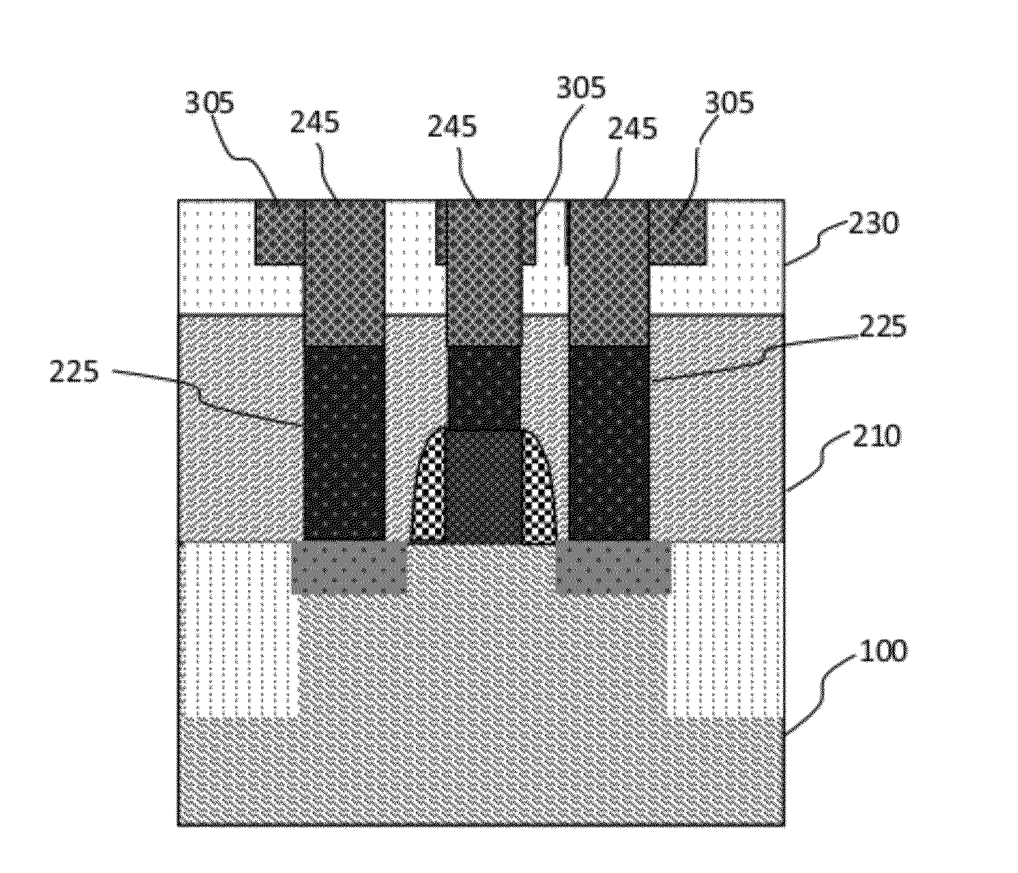
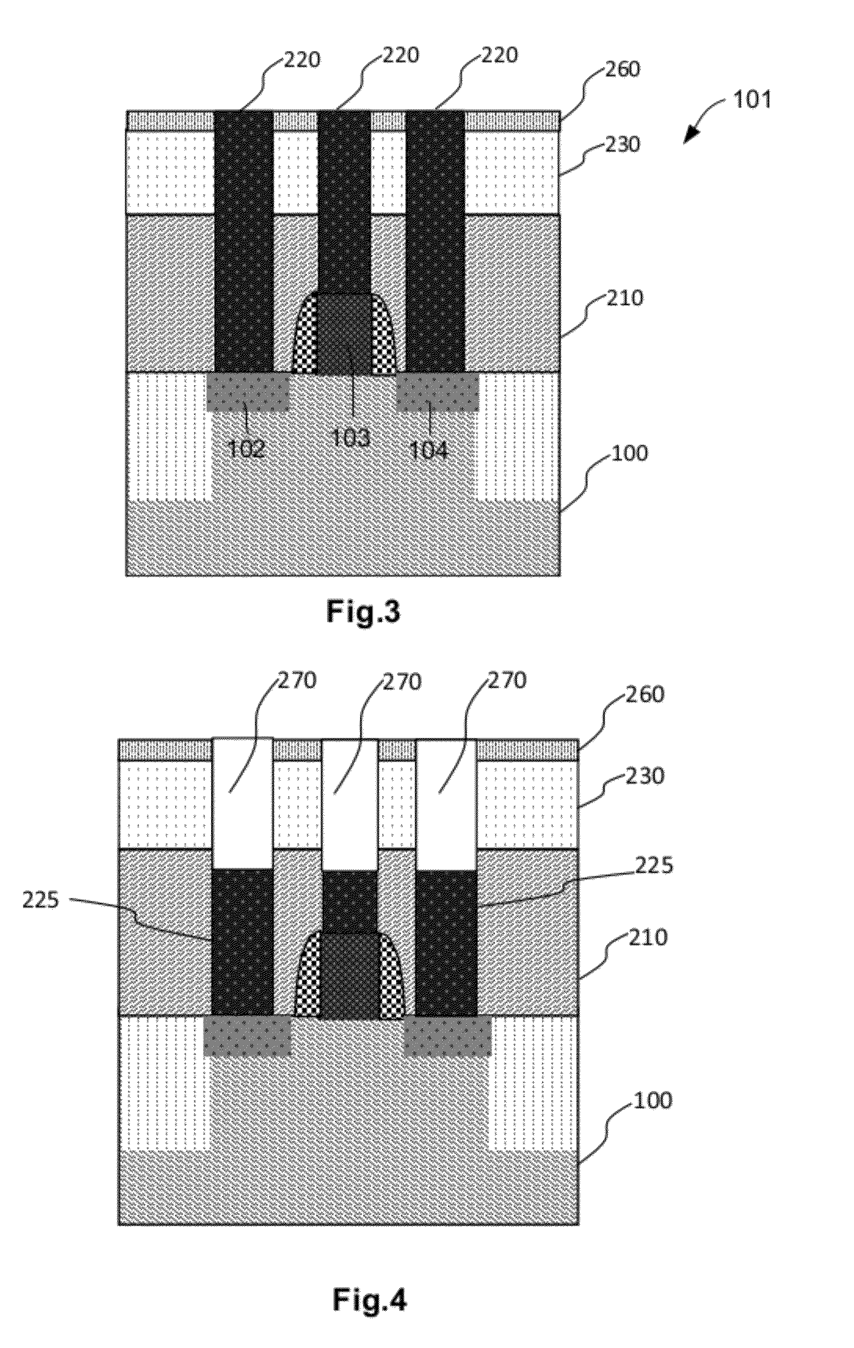
[0051]A method for manufacturing a semiconductor device according to one embodiment of the present invention and the semiconductor device manufactured thereby will be described in detail with reference to the drawings.

[0052]As shown in FIG. 3, a structure 101 comprising an interlayer dielectric layer (hereinafter abbreviated as “ILD”) 210, an ultra-low-k material layer (hereinafter abbreviated as “ULK”) 230 and a plug 220 is formed. Ultra-low-k dielectrics are defined as having a dielectric constant k of 2.7 or less.

[0053]ULK 230 is disposed on ILD 210, and ILD 210 is disposed on a substrate 100. The materials of ULK 230 and ILD 210 are known by one of ordinary skill in the relevant art. For example, ILD 210 can be formed of silicon oxide, and ULK 230 can be formed of porous SiCOH or porous macromolecule materials.

[0054]In one embodiment, a first cap layer 260 may be formed on ULK 230, so as to prevent ULK 230 from being damaged during a subsequent chemical mechanical polishing proc...


PUM


Abstract

A manufacturing method of a semiconductor device includes forming a structure comprising an interlayer dielectric layer on a substrate, an ultra-low-k material layer on the interlayer dielectric layer and a plug. The plug passes through the interlayer dielectric layer and the ultra-low-k material layer, and is formed of a first metal material. The method further includes removing an upper portion of the plug by etching to form a recessed portion, and filling the recessed portion with a second metal material. According to the method, contact-hole photolithography is performed only once, and thus avoids alignment issues that may occur when contact-hole photolithography needs to be performed twice.

Description

CROSS-REFERENCES TO RELATED APPLICATIONS[0001]This application claims priority to Chinese Patent Application No. 201110109821.5, filed on Apr. 29, 2011 entitled “Semiconductor Device and Manufacturing Method Thereof”, which is incorporated herein by reference in its entirety.BACKGROUND OF THE INVENTION[0002]1. Field of the Invention[0003]The present invention relates to semiconductor manufacturing techniques, and more specifically, relates to a semiconductor device and a manufacturing method thereof.[0004]2. Description of the Related Art[0005]With the improvement of semiconductor manufacturing techniques, critical dimensions of a semiconductor device continue to scale down. In such cases, characteristics (e.g., contact resistance) of a contact has a great impact on device performance (such as, drive current Ion degradation).[0006]When metals are used for forming a contact plug between metal wiring layers, it is necessary to select metal materials according to actual requirements, s...

Claims


Application Information

Patent Timeline
IPC IPC(8): H01L29/772H01L21/768
CPCH01L23/485H01L21/76807H01L21/76808H01L21/76847H01L2924/0002H01L2924/00H01L21/76877
Inventor HONG, ZHONGSHAN
Owner SEMICON MFG INT (SHANGHAI) CORP
Why Eureka
Try Eureka