
Metal oxide structures, devices, and fabrication methods

a metal oxide and semiconductor technology, applied in the field of lithium-containing metal oxide semiconductor compositions, can solve the problems of difficult fabrication of p-type oxide semiconductors, many impractical use, and limitation of such materials

Inactive Publication Date: 2012-11-08
GEORGIA TECH RES CORP
View PDF10 Cites 52 Cited by
  • Summary
  • Abstract
  • Description
  • Claims
  • Application Information

AI Technical Summary

Benefits of technology

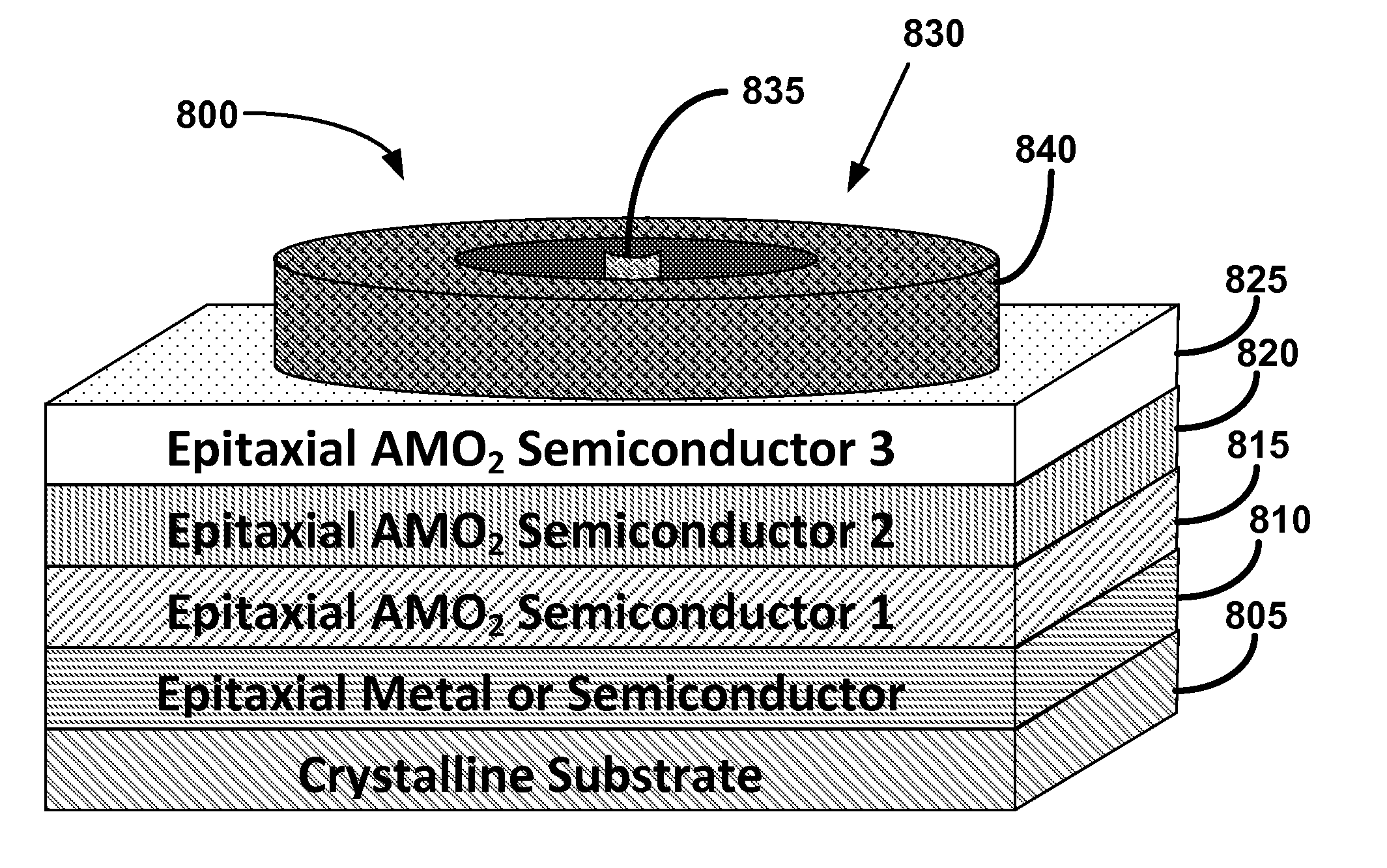
[0023]Still yet other semiconductor embodiments can generally include a crystalline substrate and an array variable resistance pillars. The crystalline substrate and a plurality of electrodes can be spaced apart from the crystalline substrate. The array of variable resistance pillars can be disposed between the crystalline substrate and at least one of the electrodes. The array of variable resistance pillars can each comprise at least two layers of epitaxial-metal-oxide semiconductor materials. The semiconductor materials can comprise metal oxide compositions enabling ion / dopant flux through the variable resistance pillars in response to an electric potential. The variable resistance pillars can retain a resistance value as a function of charge associated with the electric potential. Each of the variable resistance pillars can form part of a memory cell, memristor, memdiode, memtransistor, or charge storage device. A semiconductor device can also comprise a network of read / write access lines configured to be in communication with each of the array of variable resistance pillars to enable detection and programming of a resistance value for each of the array of variable resistance pillars.

Problems solved by technology

While ubiquitous, there are limitations with such materials.
For example, there traditionally has been a difficulty fabricating oxide semiconductors that are p-type.
Of the p-type oxide semiconductors that are known, many are impractical for use as a result of their low conductivities, low carrier concentrations, low carrier mobilities, and / or high manufacturing costs.

Method used


Image

  • Metal oxide structures, devices, and fabrication methods
  • Metal oxide structures, devices, and fabrication methods
  • Metal oxide structures, devices, and fabrication methods

Examples


Embodiment Construction

[0053]Embodiments of the present invention generally include novel metal oxide materials and a variety of devices incorporating the materials. The oxide materials include compositions, films, and methods of fabricating the materials. The materials can be used to implement and make a variety of devices. Devices and end uses include, for example, but are not limited to, memristors, neuromorphic computing, photoelectrolytic-hydrogen-generator cells, solar cells, batteries, memory cells, semiconductor devices, transistors, and devices that combine any number of these functions such as battery storage solar cells and transistors with inherent memory.

[0054]For ease of discussion, the detailed description section of the application is broken into several sections to discuss the novel materials, fabrication methods, and devices. Several of these sections also include disclosure on various applications of implementing the novel materials which are included within the broad scope of this disc...


PUM


Abstract

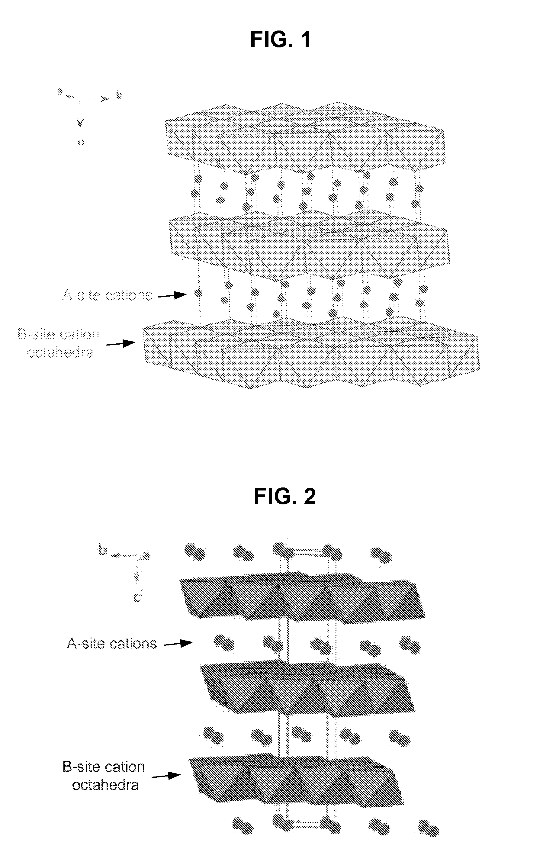
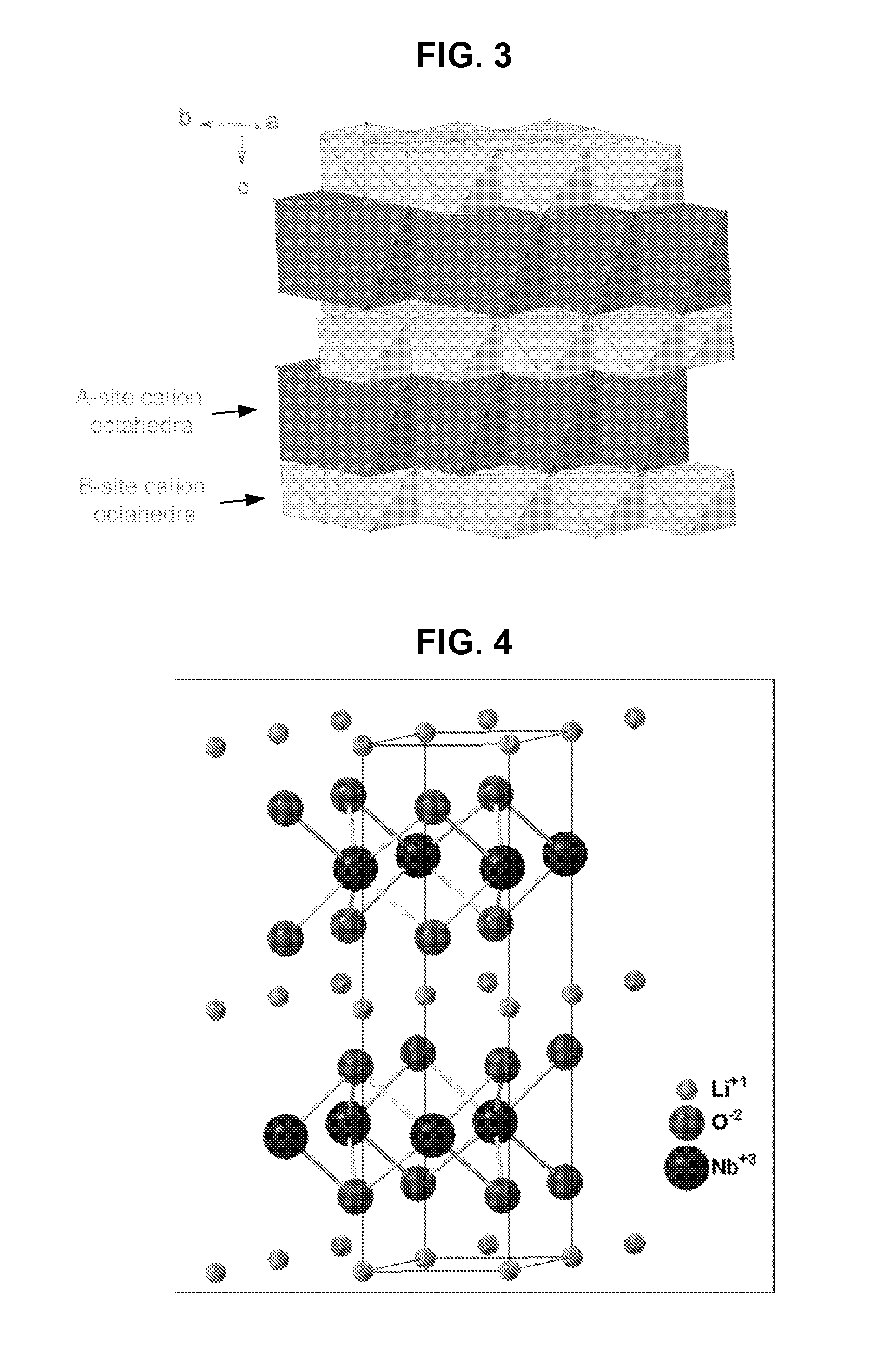
Metal oxide structures, devices, and fabrication methods are provided. In addition, applications of such structures, devices, and methods are provided. In some embodiments, an oxide material can include a substrate and a single-crystal epitaxial layer of an oxide composition disposed on a surface of the substrate, where the oxide composition is represented by ABO2 such that A is a lithium cation, B is a cation selected from the group consisting of trivalent transition metal cations, trivalent lanthanide cations, trivalent actinide cations, trivalent p-block cations, and combinations thereof, and O is an oxygen anion. The unit cell of crystal structure of the oxide composition can be characterized by first layer of a plane of lithium cations and a second layer of a plurality of edge-sharing octahedra having a B cation positioned in a center of each octahedron and an oxygen anion at each corner of each octahedron. The first layer and the second layer of the unit cell are alternatingly stacked along one axis of the unit cell. Other aspects, features, and embodiments are also claimed and described.

Description

CROSS REFERENCE TO RELATED APPLICATIONS & PRIORITY CLAIMS[0001]This application claims the benefit of and priority to U.S. Provisional Patent Application Ser. Nos. 61 / 220,366 (filed 25 Jun. 2009) and 61 / 355,495 (filed 16 Jun. 2010) both of which are incorporated by reference herein as if fully set forth below in their entireties.TECHNICAL FIELD[0002]Various embodiments of the present invention relate generally to semiconductor materials. Some of the various embodiments of the present invention more particularly relate to lithium-containing metal oxide semiconductor compositions, methods of fabricating such compositions, and end-product applications and devices incorporating these compositions.BACKGROUND[0003]Metal oxides are employed in a variety of applications owing to their ability to adopt unusual structures, which can result in beneficial chemical and / or physical characteristics. For example, layered oxide structures exhibit a wide variety of important technological uses becaus...

Claims


Application Information

Patent Timeline
IPC IPC(8): H01L29/12H01L21/20
CPCC01G33/00H02S40/38C01G51/006C01G51/42C01G53/006C01P2002/72C01P2002/78C01P2004/04C01P2006/40C25B1/003C30B23/02C30B25/02C30B29/22C30B29/30H01L21/02565H01L21/0262H01L27/101H01L27/1021H01L27/2463H01L29/1054H01L29/24H01L29/78H01L29/8615H01L31/032H01L45/085H01L45/1226H01L45/1233H01L45/147H01L45/1625H01M14/005C01G49/0027Y02E10/50Y02P20/133Y02E70/30C25B1/55H10B63/80H10N70/245H10N70/823H10N70/8836H10N70/026H10N70/826H10N70/24H10N70/253
Inventor DOOLITTLE, W. ALANCARVER, ALEXANDER G.HENDERSON, WALTER
Owner GEORGIA TECH RES CORP
Learn More