Method of manufacturing semiconductor device

a manufacturing method and semiconductor technology, applied in the direction of semiconductor devices, electrical apparatus, transistors, etc., can solve the problems of insufficient reliability of electrical, light bias test, or the like of transistors including oxide semiconductors, and achieve the effect of high field-effect mobility

Inactive Publication Date: 2012-11-15
SEMICON ENERGY LAB CO LTD
View PDF2 Cites 32 Cited by
  • Summary
  • Abstract
  • Description
  • Claims
  • Application Information

AI Technical Summary

Benefits of technology

[0013]There is a possibility of application of a transistor including an oxide semiconductor to a semiconductor device in which a transistor needs to have high field-effect mobility.

Problems solved by technology

However, transistors including oxide semiconductors, whose electrical characteristics can be changed by a bias-temperature (BT) test, a light bias test, or the like, are not sufficiently reliable.

Method used


Image

  • Method of manufacturing semiconductor device
  • Method of manufacturing semiconductor device
  • Method of manufacturing semiconductor device

Examples


embodiment 1

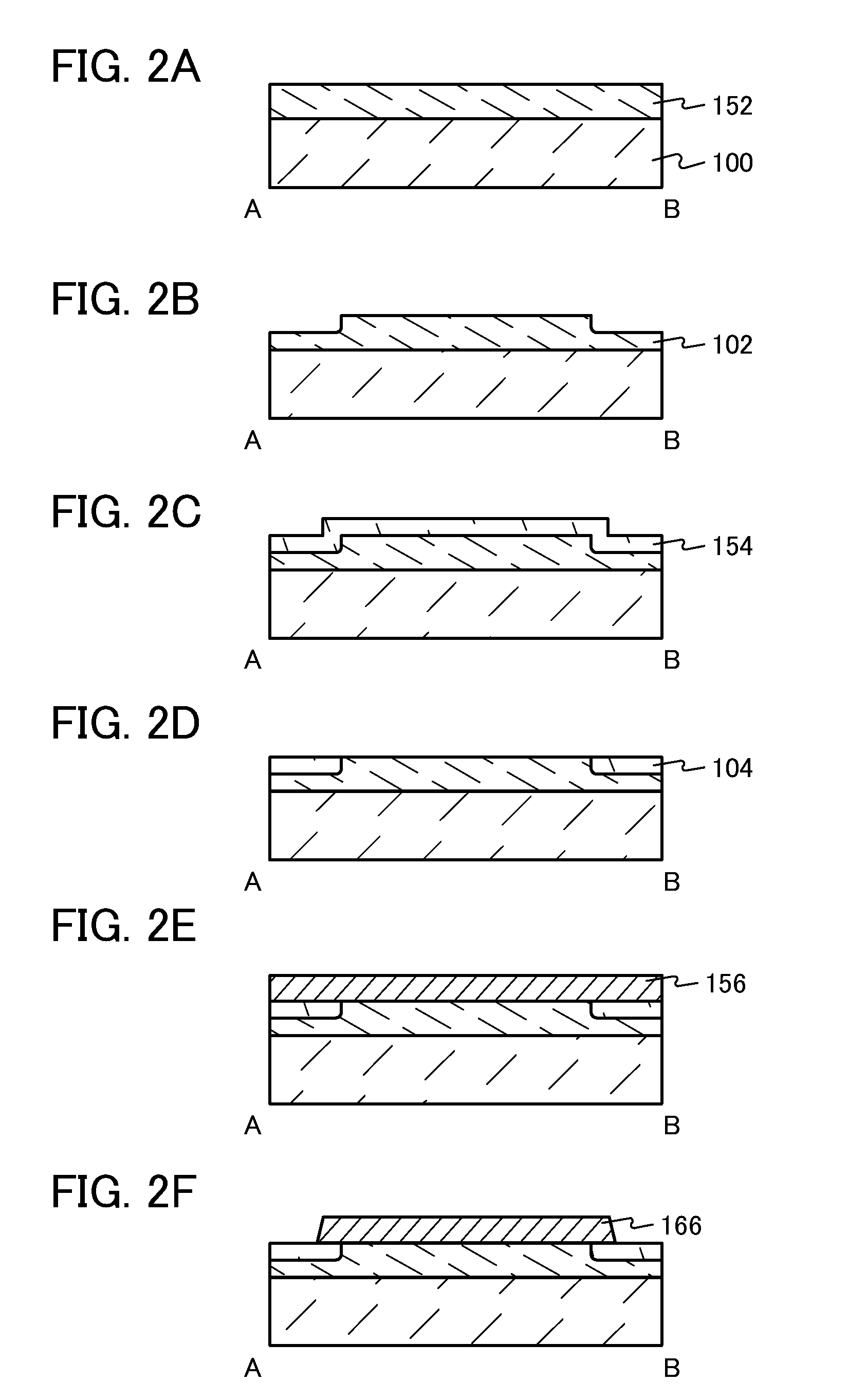
[0084]In this embodiment, an example of a transistor which is one embodiment of the present invention will be described with reference to FIGS. 1A and 1B, FIGS. 2A to 2F, FIGS. 3A to 3D, FIGS. 4A to 4C, and the like.

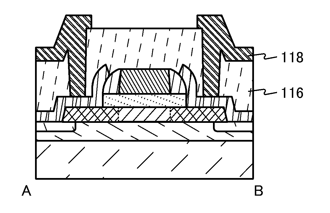
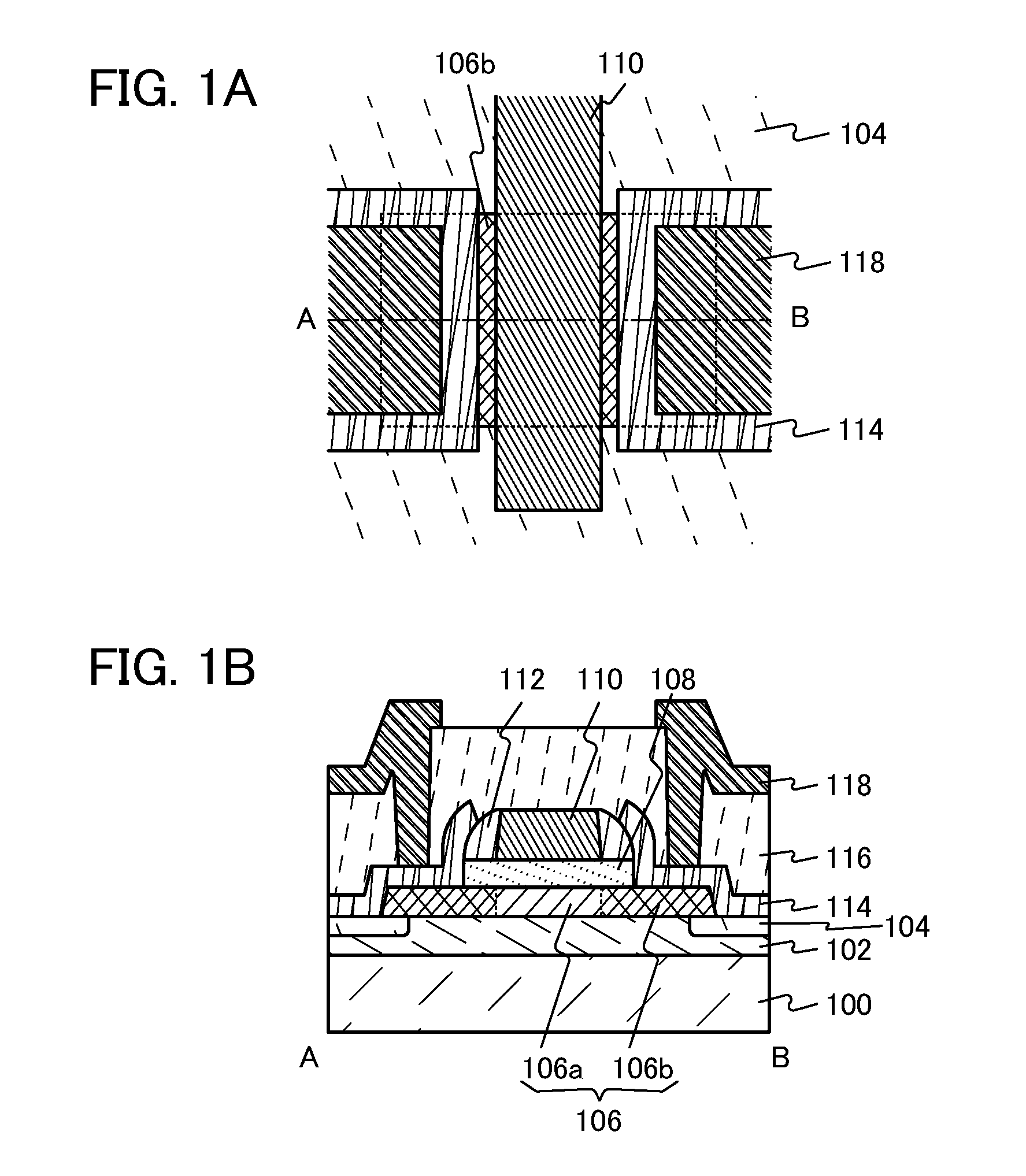
[0085]FIGS. 1A and 1B are a top view and a cross-sectional view of a transistor having a top-gate top-contact structure. FIG. 1A is the top view of the transistor. FIG. 1B shows a cross-section A-B along dashed-dotted line A-B in FIG. 1A.

[0086]The transistor illustrated in FIG. 1B includes a base insulating film 102 provided over a substrate 100; a protective insulating film 104 provided in the periphery of the base insulating film 102; an oxide semiconductor film 106 provided over the base insulating film 102 and the protective insulating film 104 and including a high-resistance region 106a and low-resistance regions 106b; a gate insulating film 108 provided over the oxide semiconductor film 106; a gate electrode 110 provided to overlap with the oxide semiconductor film...

embodiment 2

[0205]In this embodiment, a transistor whose structure is different from the structure of the transistor in Embodiment 1 is described with reference to FIGS. 5A and 5B, FIGS. 6A to 6F, and FIGS. 7A to 7C.

[0206]FIGS. 5A and 5B are a top view and a cross-sectional view of a transistor having a top-gate bottom-contact structure. FIG. 5A is the top view of the transistor. FIG. 5B shows a cross-section A-B along dashed-dotted line A-B in FIG. 5A.

[0207]The transistor illustrated in FIG. 5B includes a substrate 200, a base insulating film 202 provided over the substrate 200, a pair of electrodes 214 provided in groove portions of the base insulating film 202, an oxide semiconductor film 206 which includes a high-resistance region 206a and low-resistance regions 206b and which is provided over the base insulating film 202 and the pair of electrodes 214, a gate insulating film 208 provided over the oxide semiconductor film 206, a gate electrode 210 provided to overlap with the oxide semicond...

embodiment 3

[0225]In this embodiment, an example of manufacturing a memory that is a semiconductor device with the use of the transistor described in Embodiment 1 or 2 will be described.

[0226]Typical examples of volatile memories include a dynamic random access memory (DRAM) which stores data by selecting a transistor included in a memory element and storing electric charge in a capacitor and a static random access memory (SRAM) which holds stored data using a circuit such as a flip-flop.

[0227]The transistor described in Embodiment 1 or 2 can be applied to some of transistors included in the memory.

[0228]For example, an example of a DRAM that is a semiconductor device to which the transistor described in Embodiment 1 is applied is described with reference to FIGS. 8A to 8C.

[0229]FIG. 8A is a cross-sectional view of the DRAM. A transistor 340 includes the substrate 100, the base insulating film 102 provided over the substrate 100, the protective insulating film 104 provided in the periphery of t...


PUM


Abstract

A highly reliable transistor which includes an oxide semiconductor and has high field-effect mobility and in which a variation in threshold voltage is small is provided. By using the transistor, a high-performance semiconductor device, which has been difficult to realize, is provided. The transistor includes an oxide semiconductor film which contains two or more kinds, preferably three or more kinds of elements selected from indium, tin, zinc, and aluminum. The oxide semiconductor film is formed in a state where a substrate is heated. Further, oxygen is supplied to the oxide semiconductor film with an adjacent insulating film and / or by ion implantation in a manufacturing process of the transistor, so that oxygen deficiency which generates a carrier is reduced as much as possible. In addition, the oxide semiconductor film is highly purified in the manufacturing process of the transistor, so that the concentration of hydrogen is made extremely low.

Description

BACKGROUND OF THE INVENTION[0001]1. Field of the Invention[0002]The present invention relates to a semiconductor device including a semiconductor element such as a transistor which includes an oxide semiconductor, and a method for manufacturing the semiconductor device.[0003]In this specification, a semiconductor device generally refers to a device which can function by utilizing semiconductor characteristics; an electro-optical device, a light-emitting display device, and an electronic device are all included in the category of the semiconductor device.[0004]2. Description of the Related Art[0005]Many transistors formed over a glass substrate or the like are manufactured using amorphous silicon, polycrystalline silicon, or the like, as typically seen in liquid crystal display devices. Although a transistor manufactured using amorphous silicon has low field-effect mobility, it can be formed over a larger glass substrate. On the other hand, although a transistor manufactured using po...

Claims


Application Information

Patent Timeline
Patent Type & Authority Applications(United States)
IPC IPC(8): H01L29/786H01L21/34
CPCH01L21/0242H01L21/02554H01L21/02565H01L21/02595H01L21/84H01L27/10873H01L29/66742H01L27/1203H01L29/78603H01L29/7869H01L29/66969H01L21/02656H01L27/1156H10B12/05H10B41/70H01L21/324H01L27/1222H01L27/1225H01L27/1255H01L29/78609
Inventor NODA, KOSEIYAMAZAKI, SHUNPEIHONDA, TATSUYASEKINE, YUSUKETOMATSU, HIROYUKI
Owner SEMICON ENERGY LAB CO LTD
Why Eureka
Try Eureka