

Semiconductor light emitting diode chip and light emitting device using the same
a technology of light-emitting diodes and semiconductors, applied in semiconductor devices, basic electric elements, electrical appliances, etc., can solve the problems of increasing the volume of products, increasing the product cost, and affecting the reflective effect of products, so as to improve the reflective effect, the reflectance of the dbr structure is considerably reduced, and the effect of high reflectan
- Summary
- Abstract
- Description
- Claims
- Application Information
AI Technical Summary
Benefits of technology
Problems solved by technology
Method used
Image

Examples
experimental example 1
Effect of DBR+Metal Reflective Film
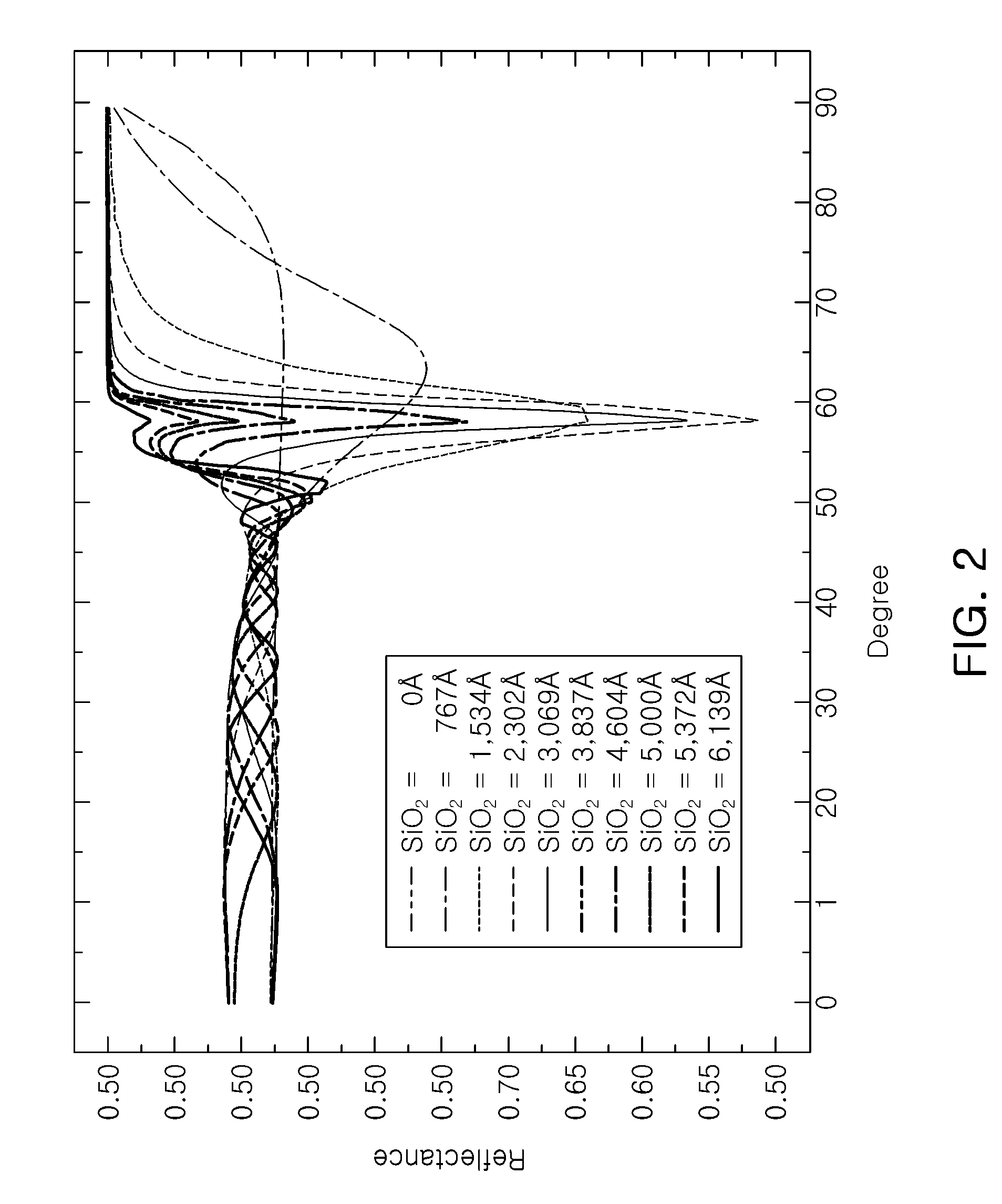
[0060]In order to confirm the improvement effect of the reflective characteristics of the DBR+metal reflective film employed in the present embodiment, two DBR reflective structures were manufactured by alternatively depositing forty eight SiO2 thin films and Si3N4 thin films (each being twenty four films).
[0061]An Al metal reflective film was additionally deposited on one face of one of the two DBR structures. Reflective characteristics of the DBR structure itself and the DBR+metal reflective structure obtained thus were measured as reflectance of each wavelength over incident angle, and FIGS. 5 and 6 show the results.
[0062]As shown in FIGS. 5 and 6, when the incident angle is small (about 50° or smaller), there is not much difference between the DBR structure and the DBR+metal reflective structure. But, in a case in which the incident angle is large, when only the DBR structure was used, its reflectance is greatly changed according to wavelength ...
experimental example 2
Effect of DBR+Metal Reflective Film
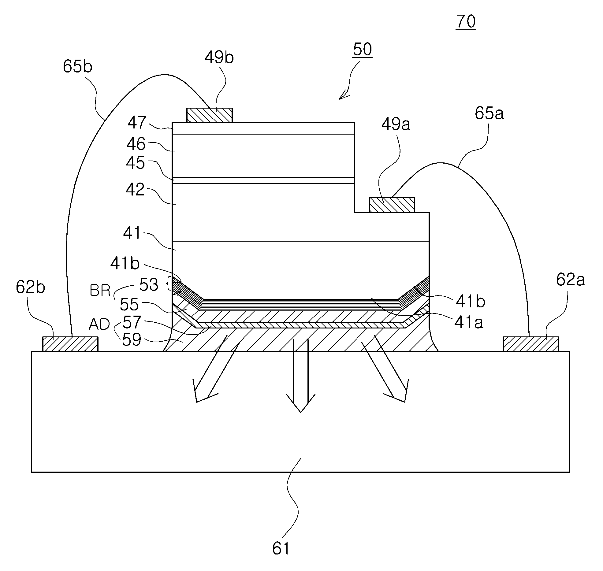
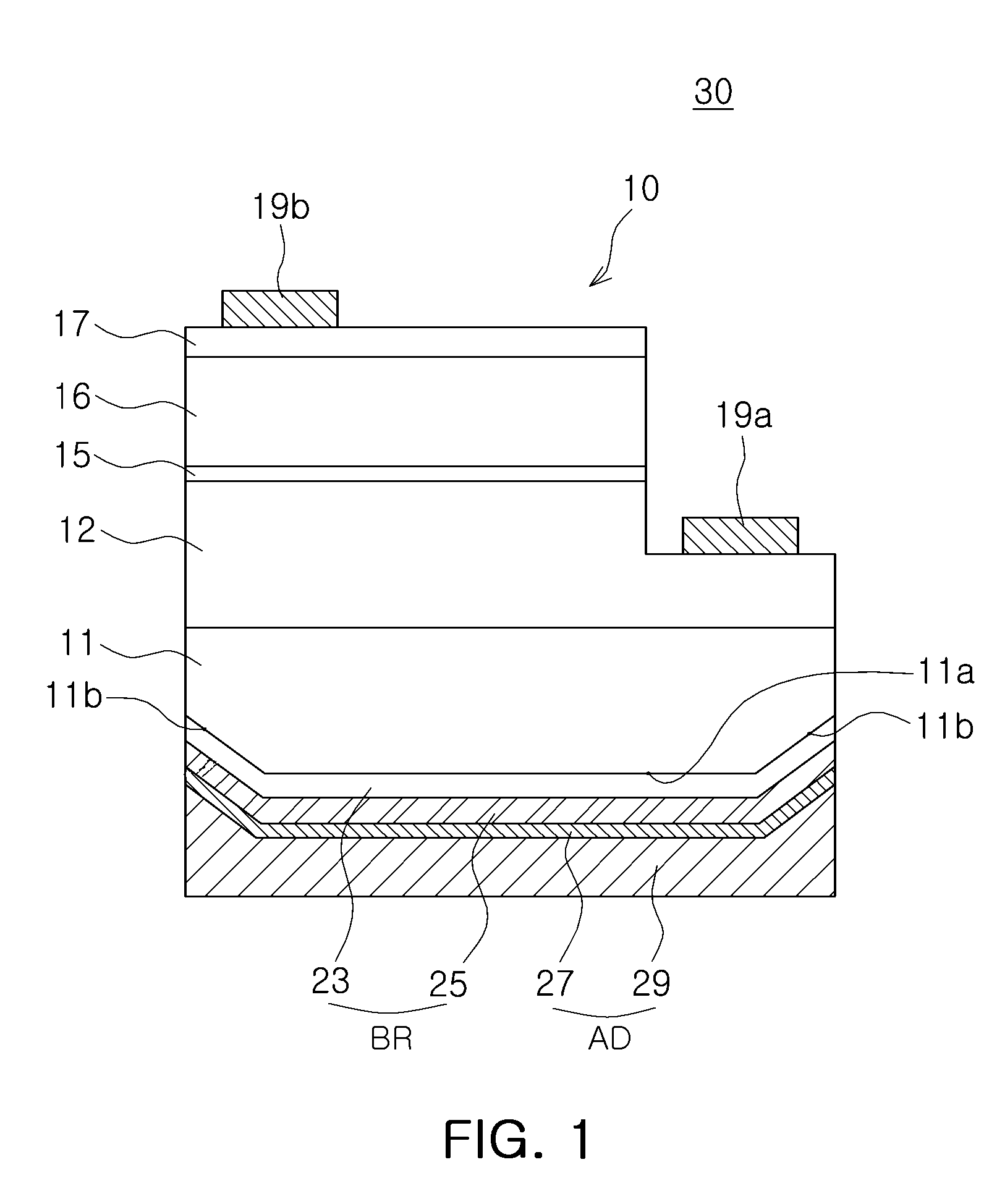
[0068]As described above, also in case in which the diffusion barrier film 57 or the eutectic metal layer 59 is directly applied without the metal reflective film 55 having high reflectance such as aluminum (Al) or silver (Ag), desired reflective characteristics can be hardly obtained, and such an effect of a package structure will now be checked through the embodiment and Comparative Example.
embodiment
[0069]The DBR structure as shown in Experiment Example 1 was formed on a lower face (including a sloped face) of a sapphire substrate of a nitride LED, and an AL metal reflective film was deposited thereon. In addition, an Au—Sn junction metal layer was formed along with a Ti / Au diffusion barrier film as a junction lamination.
[0070]The LED chip manufactured thusly was bonded to a silicon sub-mount substrate by using the junction metal layer to manufacture a light emitting device having a structure similar to that illustrated in FIG. 7.
PUM
 Abstract
Description
Claims
Application Information