Silicon carbide substrate, silicon carbide ingot, and methods for manufacturing silicon carbide substrate and silicon carbide ingot

a technology of silicon carbide and substrate, which is applied in the direction of water-setting substance layered product, polycrystalline material growth, transportation and packaging, etc., can solve the problems of lowering the utilization efficiency of substrate, and achieve the effect of light transmittance, reduced nitrogen concentration variation, and high light transmittan

Inactive Publication Date: 2012-11-22
SUMITOMO ELECTRIC IND LTD
View PDF2 Cites 6 Cited by
  • Summary
  • Abstract
  • Description
  • Claims
  • Application Information

AI Technical Summary

Benefits of technology

[0020]A silicon carbide substrate according to the present invention is obtained by slicing the silicon carbide ingot described above. Consequently, the silicon carbide substrate in which the region having a relatively low nitrogen concentration (or region having a high light transmittance) is formed in a large region including the substrate central portion can be readily obtained.
[0021]A silicon carbide substrate according to the present invention is obtained by slicing the silicon carbide ingot, after the high concentration nitrogen region was removed from the silicon carbide ingot. By removing the high concentration nitrogen region (region having a low light transmittance) in advance in this manner, the silicon carbide substrate is formed using the silicon carbide ingot including only the region having a nitrogen concentration lower than in the high concentration nitrogen region (region having a light transmittance higher than in the high concentration nitrogen region). Accordingly, the silicon carbide substrate with smaller variation in nitrogen concentration and light transmittance can be obtained.
[0022]A silicon carbide substrate according to the present invention includes a high concentration nitrogen region having a nitrogen concentration relatively higher than in a remaining portion formed at one end portion in either a <11-20> direction or a <1-100> direction. The high concentration nitrogen region may be formed at an end portion on an upstream side, the upstream side being a side where an angle of intersection between a <0001> direction axis of the silicon carbide substrate and the surface of the silicon carbide substrate in either the <11-20> direction or the <1-100> direction (off angle direction) is an acute angle. By controlling the arrangement of the (0001) facet in this manner when growing a silicon carbide ingot for forming a silicon carbide substrate, the high concentration nitrogen region can be readily arranged at the end portion of the silicon carbide substrate.

Problems solved by technology

Thus, when forming a device on the surface of the silicon carbide substrate in the region having a relatively low nitrogen concentration, the device will be formed in a region other than the high concentration nitrogen region (namely, the device will be formed in a region other than the high concentration nitrogen region and a boundary region between the high concentration nitrogen region and the low concentration nitrogen region), resulting in lowered substrate utilization efficiency.

Method used


Image

  • Silicon carbide substrate, silicon carbide ingot, and methods for manufacturing silicon carbide substrate and silicon carbide ingot
  • Silicon carbide substrate, silicon carbide ingot, and methods for manufacturing silicon carbide substrate and silicon carbide ingot
  • Silicon carbide substrate, silicon carbide ingot, and methods for manufacturing silicon carbide substrate and silicon carbide ingot

Examples


examples

[0137]To confirm the effects of the present invention, ingots and substrates were manufactured and their characteristics were measured as follows.

[0138](Samples)

[0139]Samples of a silicon carbide ingot and a silicon carbide substrate obtained by slicing the silicon carbide ingot were prepared as follows in an example and a comparative example of the present invention.

[0140]

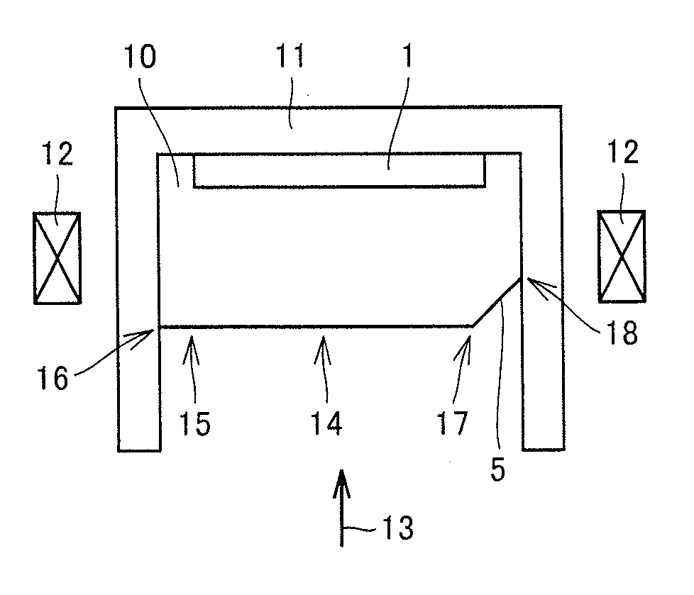
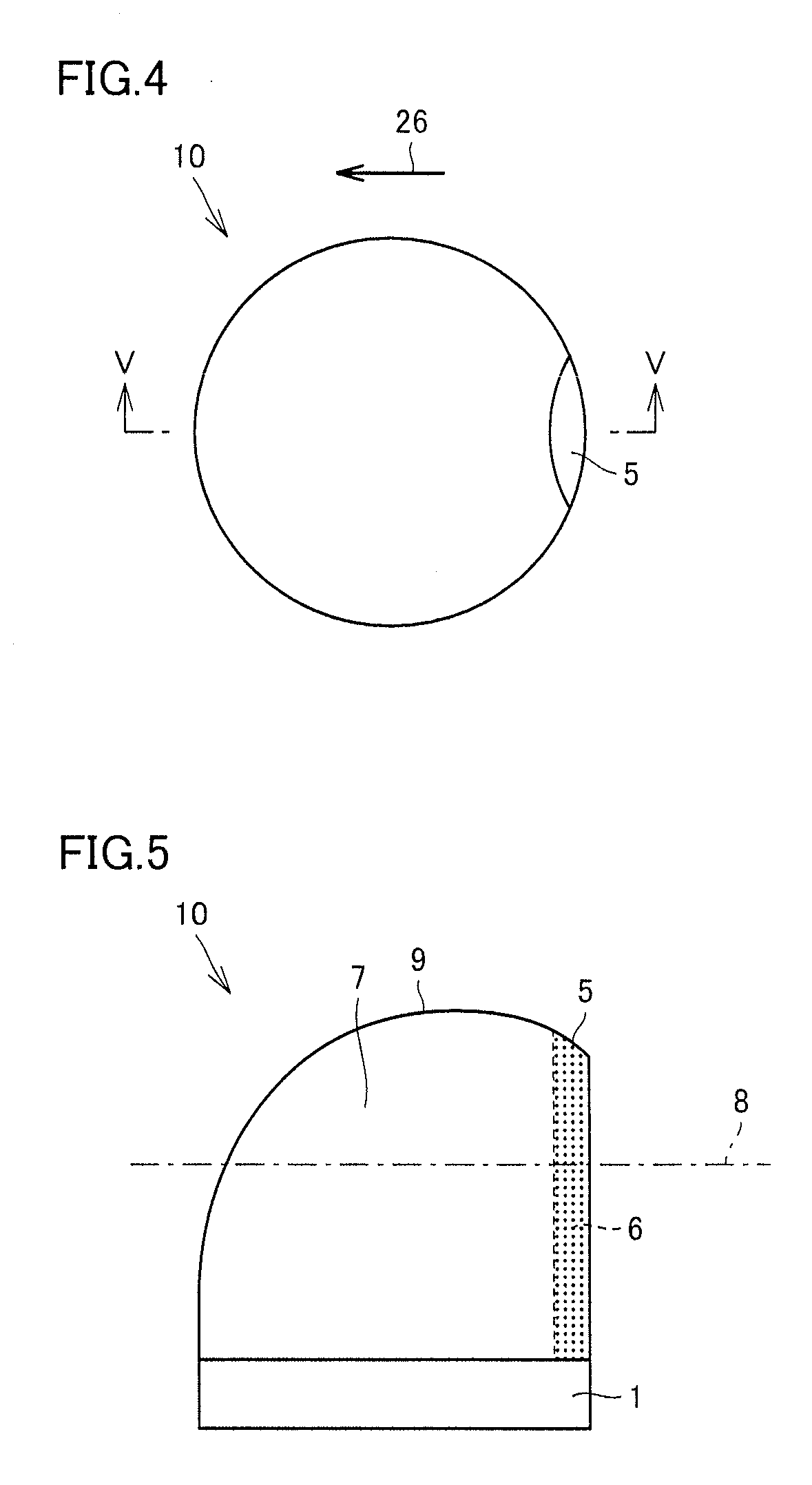
[0141]In order to manufacture silicon carbide ingots, silicon carbide single crystal substrates having the following conditions were prepared as base substrates. Specifically, in order to manufacture the ingot according to the present invention, six 4H-SiC single crystal substrates (three for the example and three for the comparative example) were prepared as base substrates 1. Base substrates 1 had a diameter of 50 to 180 mm, and a thickness of 100 to 2000 μm. Base substrates 1 had a thickness of 800 μm. Main surfaces of base substrates 1 had an off angle of 4° in the direction relative to the (0001) plane. At l...


PUM

PropertyMeasurementUnit
off angleaaaaaaaaaa
off angleaaaaaaaaaa
wavelengthaaaaaaaaaa

Abstract

A method of manufacturing a silicon carbide ingot having highly uniform characteristics includes a preparation step of preparing a base substrate made of single crystal silicon carbide and having an off angle of 0.1° or more and 10° or less in an off angle direction which is either a <11-20> direction or a <1-100> direction relative to a (0001) plane, and a film formation step of growing a silicon carbide layer on a surface of the base substrate. In the film formation step, a region having a (0001) facet 5 is formed on a surface of the grown silicon carbide layer at an end portion on an upstream side, the upstream side being a side where an angle of intersection between a <0001> direction axis of the base substrate and the surface of the base substrate in the off angle direction is an acute angle.

Description

BACKGROUND OF THE INVENTION[0001]1. Field of the Invention[0002]The present invention relates to a silicon carbide substrate, a silicon carbide ingot, and methods for manufacturing the silicon carbide substrate and the silicon carbide ingot, and more particularly to a silicon carbide substrate and a silicon carbide ingot with little variation in characteristics such as impurity concentration, and methods for manufacturing the silicon carbide substrate and the silicon carbide ingot.[0003]2. Description of the Background Art[0004]Silicon carbide (SiC) has been conventionally studied as a next-generation semiconductor material to replace silicon (Si). A conventional method of manufacturing a substrate made of silicon carbide is known, in which a silicon carbide single crystal is grown on a seed substrate to form a silicon carbide ingot, and the silicon carbide ingot is sliced to manufacture the substrate. In this method, a seed crystal is prepared with a (0001) plane (so-called c-surfa...

Claims


Application Information

Patent Timeline
Patent Type & Authority Applications(United States)
IPC IPC(8): C01B31/36B32B3/10B32B3/02C30B23/02B32B9/04
CPCC30B23/025Y10T428/21Y10T428/24322C30B29/36
Inventor SASAKI, MAKOTONISHIGUCHI, TARO
Owner SUMITOMO ELECTRIC IND LTD
Why Eureka
Try Eureka