
Three-level digital-to-analog converter

Active Publication Date: 2012-12-06
TEXAS INSTR INC
View PDF1 Cites 9 Cited by
  • Summary
  • Abstract
  • Description
  • Claims
  • Application Information

AI Technical Summary

Benefits of technology

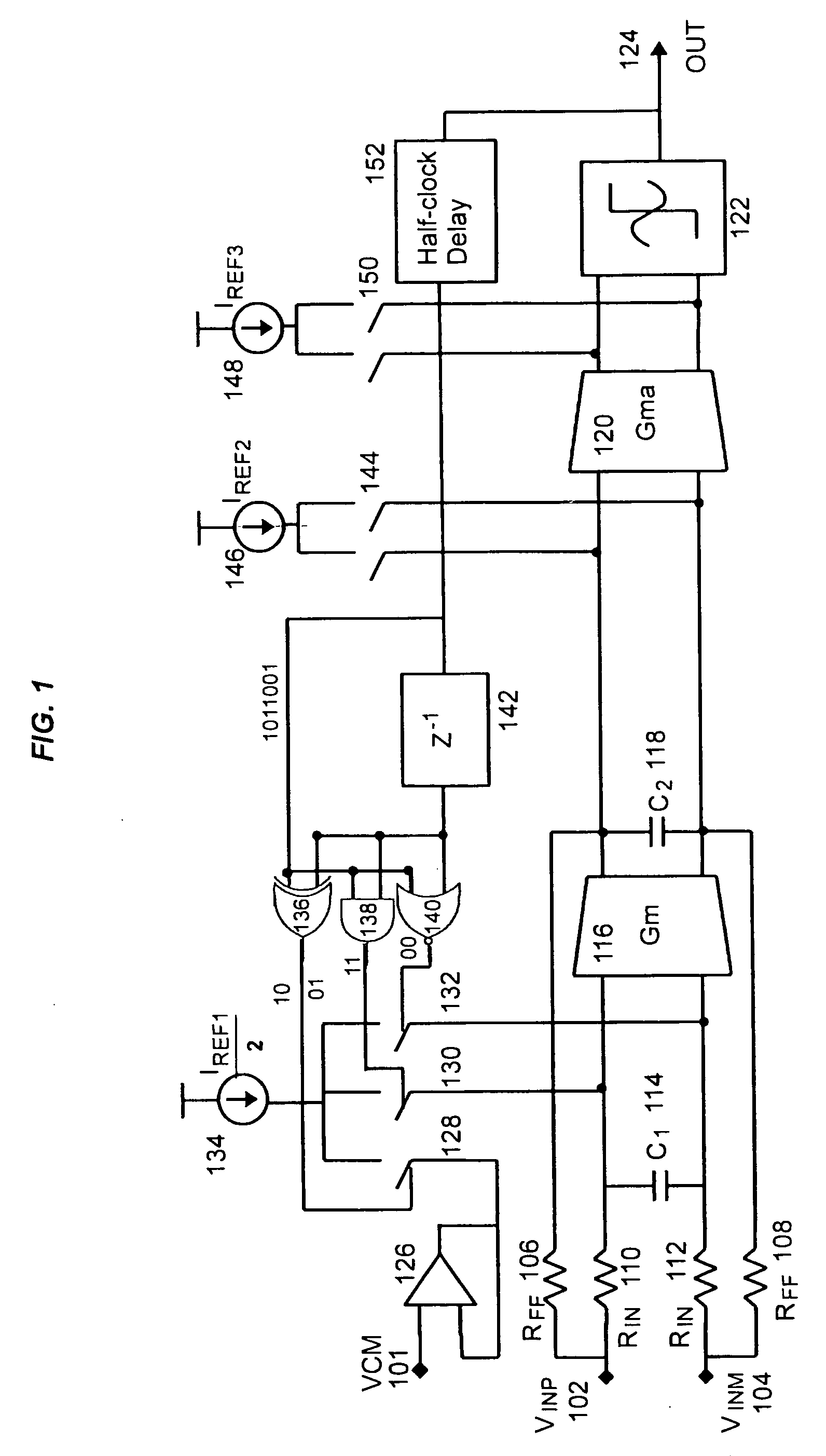
[0010]In the closed-loop configuration, a system for processing a signal includes a receiver configured to receive an input analog signal having a positive input and a minus input; a converter configured to quantize the input analog signal into a two-level output stream; a summing junction configured to selectively couple a current source to one of the minus input, the positive input, and a current sink; and a signal generator configured to generate a three-level control signal based on the two-level output stream to control operation of the summing junction. Thus, when adjacent values of the output stream of the quantizer are different, the current source can be coupled to a current sink instead of one of the signal inputs. In both an open-loop and closed-loop configuration, this architecture provides a significantly reduced noise floor.

Problems solved by technology

One of the major limitations in high fidelity low power audio design, such as for headsets, is thermal noise of the DAC components.
Because of this, in order to provide acceptable idle channel noise characteristics, the DAC device is usually relatively large that leads to inefficient use of chip space and high power consumption.
However, this solution introduces a number of issues.
Mismatch between PMOS and NMOS devices creates significant linearity issues that affect the overall chain and the subsequent amplifier design.
Additionally, using NMOS devices makes it more difficult to isolate noise.
APSDM ADCs are subject to resistor and capacitor absolute value variances and excess loop delay and parasitic poles.
Variances in resistor and capacitor absolute value tend to cause large absolute ADC gain variations and the movement of poles and zeros, which degrades performance and stability.
Further, a loop delay compensation circuit may be required to reduce sensitivity to quantizer metastability, latch clock-to-Q time, and feedback DAC propagation delay.
This requires additional circuits for level-shifting, which consume additional chip area and power.
The undesired result is that the noise of the first stage integrator (passive) is referred back to the input stage and, as a result, amplified.
Thus, the noise floor of the APSDM is limited.

Method used


Image

  • Three-level digital-to-analog converter
  • Three-level digital-to-analog converter
  • Three-level digital-to-analog converter

Examples


Embodiment Construction

[0017]The detailed description set forth below in connection with the appended drawings is intended as a description of various embodiments of the invention and is not intended to represent the only embodiments in which the invention may be practiced. The detailed description includes specific details for the purpose of providing a thorough understanding of the invention. However, it will be apparent to those skilled in the art that the invention may be practiced without these specific details. In some instances, well known structures and components are shown in block diagram form in order to avoid obscuring the concepts of the invention.

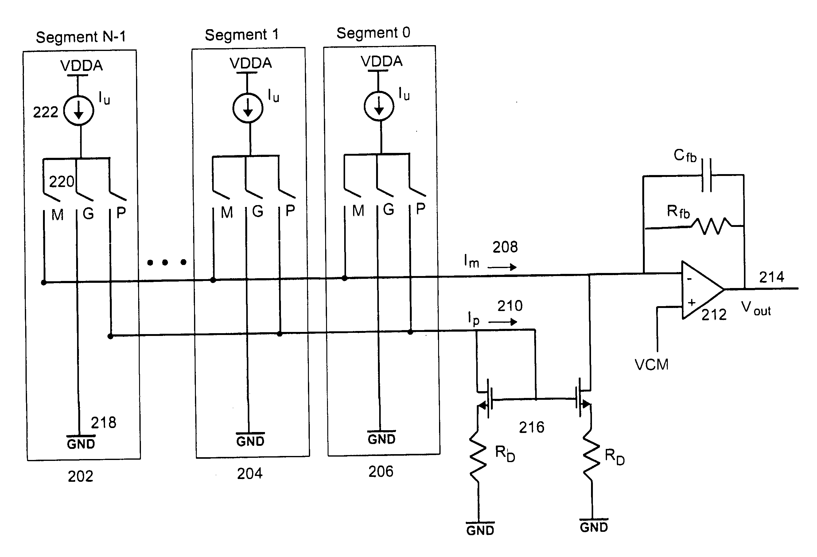
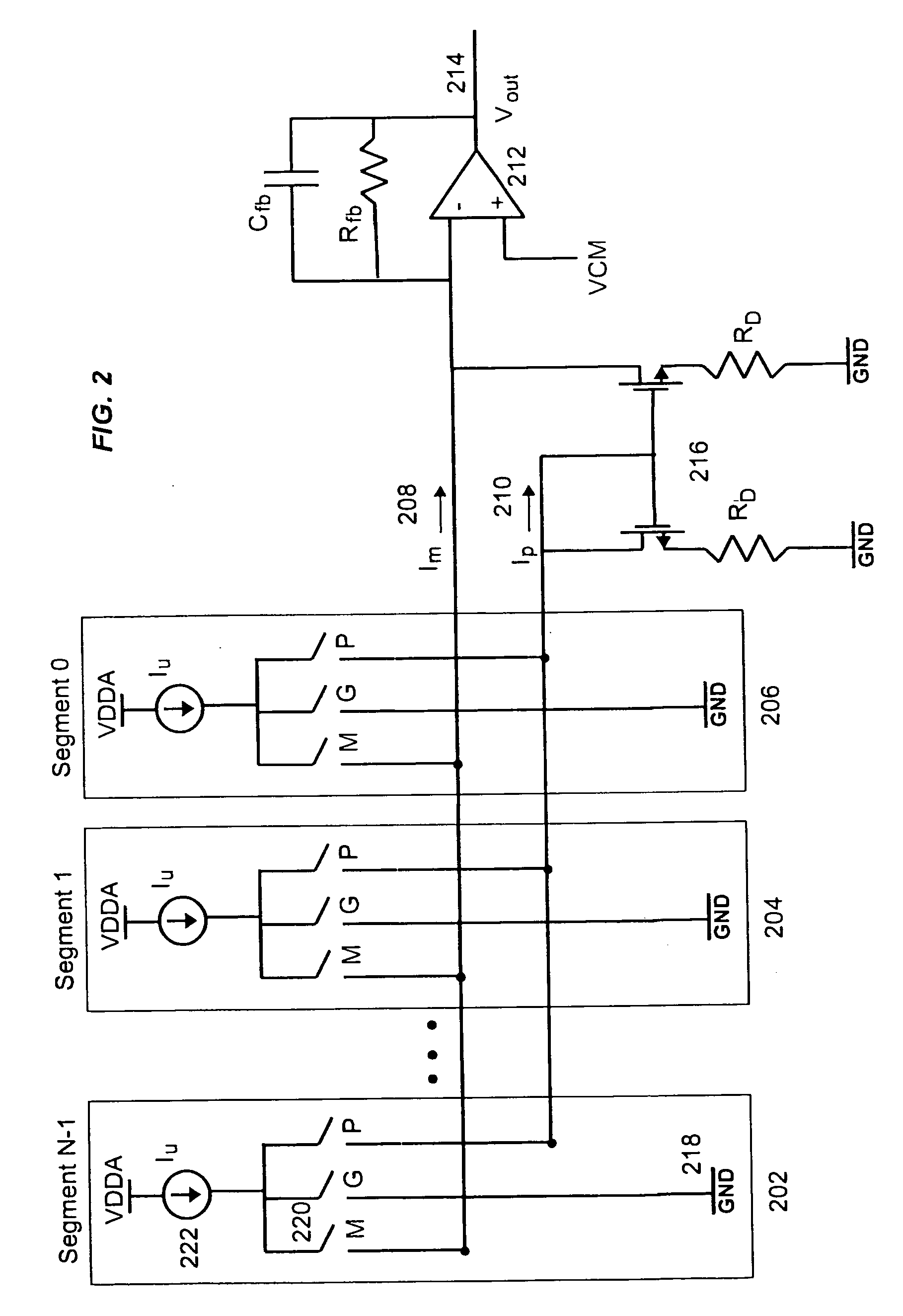
[0018]A three-level digital-to-analog converter is described in two different configurations. The first configuration is with respect to FIG. 1. In this configuration, the DAC is part of the feedback loop of an analog-to-digital converter. The second configuration is with respect to FIGS. 2 and 3 and illustrates an open-loop configuration of the thr...


PUM


Abstract

A system for processing a signal includes a detector configured to detect a two-level stream of bits; a converter configured to generate a three-level control signal based on two adjacent values within the two-level stream of bits; and a switch configured to determine which of three different paths to couple a current source to based on a value of the three-level control signal. Thus, based on adjacent values of the output stream a three-level control signal is generated which controls coupling of the current source to one of three different paths. This type of three-level digital-to-analog converter can be, for example, part of the feedback loop of an analog-to-digital converter. Similar techniques can also be utilized in a multi-segment digital-to-analog converter in which each segment of the DAC is controlled by a 3-level control signal and the DAC is implement using PMOS devices. The current source for each DAC segment is diverted to ground, the M-node, or the P-node depending on the value of the 3-level control signal.

Description

BACKGROUND[0001]1. Field[0002]The present invention relates generally to signal processing and, more particularly, to digital to analog conversion.[0003]2. Description of Related Art[0004]One of the major limitations in high fidelity low power audio design, such as for headsets, is thermal noise of the DAC components. In a typical DAC design, thermal noise is a fixed value once the maximum output voltage and load requirements are determined. DAC output referred thermal noise at the driver output does not change even if the signal swing is reduced. Because of this, in order to provide acceptable idle channel noise characteristics, the DAC device is usually relatively large that leads to inefficient use of chip space and high power consumption.[0005]One attempt at a solution is to provide a three-level digital-to-analog converter using both PMOS and NMOS devices as matched current cources. However, this solution introduces a number of issues. For example, there must be almost perfect ...

Claims


Application Information

Patent Timeline
IPC IPC(8): H03M1/72
CPCH03M1/747H03M1/66H03M3/464
Inventor HEZAR, RAHMIHAROUN, BAHERKIPER, HALILFARES, MOUNIRKUMAR, AJAY
Owner TEXAS INSTR INC
Learn More