Method and system for manufacturing liquid crystal display device

Inactive Publication Date: 2012-12-13
NITTO DENKO CORP
View PDF1 Cites 11 Cited by
  • Summary
  • Abstract
  • Description
  • Claims
  • Application Information

AI Technical Summary

Benefits of technology

[0012]According to this feature, optical films are bonded alternately to the first and second panel surfaces of a liquid crystal panel, which can reduce warping of the liquid cry

Problems solved by technology

In such a case, the successive bonding to the back side increases the shrinking force generated on the back side, so that the shrinking forces on the first and second panel surfaces of the liquid crystal panel become out of balance, which changes the amount of warping.
Therefore, if more optical films are bonded to one panel surface of a liquid crystal panel in an unbalanced manner, the liquid crystal panel will be warped significantly, so that the end of the liquid

Method used


Image

  • Method and system for manufacturing liquid crystal display device
  • Method and system for manufacturing liquid crystal display device
  • Method and system for manufacturing liquid crystal display device

Examples


embodiment 1

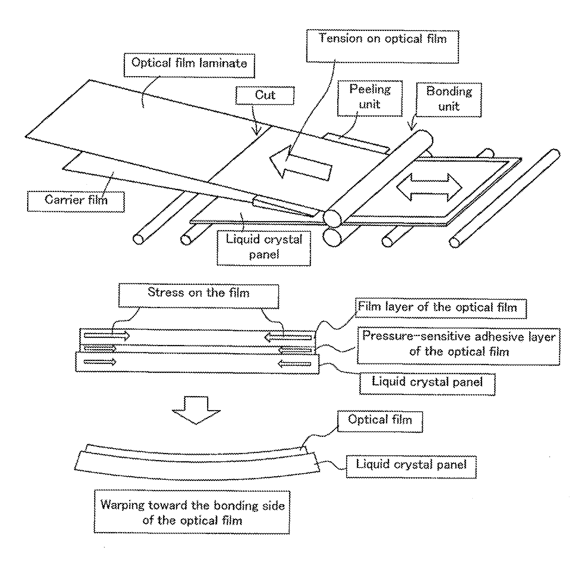
[0032](Method for Manufacturing Liquid Crystal Display Device)

[0033]The liquid crystal display device manufacturing method includes: feeding long carrier films from continuous rolls, respectively, wherein the continuous rolls include rolls of laminates including the long carrier films and pressure-sensitive adhesive-carrying optical films each with a specific width placed on the carrier films; and bonding steps including bonding the optical films, which are peeled off or being peeled off from the carrier films, to first and second panel surfaces of a liquid crystal panel, respectively, wherein in the bonding steps, bonding the optical film to the first panel surface of the liquid crystal panel and bonding the optical film to the second panel surface of the liquid crystal panel are performed alternately.

[0034]The process until the bonding steps includes carrier film feeding steps including feeding the carrier films from the continuous rolls, respectively, and peeling steps including ...

examples

[0059]Different optical films were bonded to a liquid crystal panel (32 inch size) using the sheet piece lamination apparatuses shown in FIG. 4. The manufacturing system was configured to perform the turnover and 90° rotation of the liquid crystal panel appropriately depending on the optical film type and the bonding order. When long optical films are cut into sheet pieces, the sizes of the sheet pieces are determined depending on the bonding side and the bonding direction.

[0060]The optical films used were a MD polarizing film (SEG1423DU manufactured by NITTO DENKO CORPORATION), an anti-glare-treated AGS film (AGS1 (TDP1490) (product name), manufactured by Dai Nippon Printing Co., Ltd.), and a reflective polarizing film (DBEF manufactured by 3M Company). Table 1 shows the conditions concerning the optical films and the liquid crystal panel surface subjected to bonding (back side or viewer side) in Examples and Comparative Examples, respectively. In Table 1, sections (1) to (3) are e...


PUM


Abstract

Provided are a method and a system for manufacturing a liquid crystal display device, which can reduce warping of a liquid crystal panel by bonding optical films alternately to the first and second panel surfaces of the liquid crystal panel, in which the method includes: feeding carrier films from continuous rolls, respectively; and bonding steps including bonding optical films, which are peeled off or being peeled off from the carrier films, to the first and second panel surfaces of a liquid crystal panel, respectively, wherein in the bonding steps, bonding the optical film to the first panel surface of the liquid crystal panel and bonding the optical film to the second panel surface of the liquid crystal panel are performed alternately.

Description

BACKGROUND OF THE INVENTION[0001]1. Field of the Invention[0002]The invention relates to a method and a system for manufacturing a liquid crystal display device.[0003]2. Description of the Related Art[0004]A conventional process of laminating optical films to a liquid crystal panel includes cutting an optical film into pieces and bonding a cut piece of the optical film (a sheet piece) to the liquid crystal panel. In such a bonding process, very low and stable tension can be applied to the optical film, and therefore, the liquid crystal panel is less likely to be warped due to variations in tension or over-tension after the bonding. In recent years, a bonding apparatus capable of simultaneously bonding pieces of optical film to both sides of a liquid crystal panel have been developed, which makes it easy to provide more uniform bonded states on the front and back sides in the bonding process.[0005]On the other hand, a process is known which includes drawing a carrier film from a cont...

Claims


Application Information

Patent Timeline
IPC IPC(8): B32B37/20B32B37/12
CPCB32B37/0015B32B37/02B32B37/185B32B38/18Y10T156/1705G02F1/1303G02F1/1333G02F1/133528G02F2202/28B32B2457/202G02B5/30G02F1/1335
Inventor HIRATA, SATOSHIKONDO, SEIJI
Owner NITTO DENKO CORP
Why Eureka
Try Eureka