Module substrate, module-substrate manufacturing method, and terminal connection substrate

Active Publication Date: 2012-12-20
MURATA MFG CO LTD
View PDF4 Cites 19 Cited by
  • Summary
  • Abstract
  • Description
  • Claims
  • Application Information

AI Technical Summary

Benefits of technology

[0049]With the above configuration, electrical connection can be made using not a thin plating film formed in a through hole but the columnar terminal electrodes, and thus a relatively large current can be passed. A complicated step, such as forming a through hole and forming a plating film, is not necessary, the manufacturing steps can be simplified, and thus the manufacturing cost as a whole can be reduced.
[0050]With the above configuration, because a coupling plate by which a plurality of terminal electrodes is integrated does not exist, a step of grinding the coupling plate is not n

Problems solved by technology

Accordingly, there is a problem in that it is difficult to reduce the manufacturing cost.
In addition, if the coupling plate was not able to be sufficiently ground, poor connections may occur in the connection electrodes.
In the module disclosed in Japanese Unexamined Patent Application Publicat

Method used


Image

  • Module substrate, module-substrate manufacturing method, and terminal connection substrate
  • Module substrate, module-substrate manufacturing method, and terminal connection substrate
  • Module substrate, module-substrate manufacturing method, and terminal connection substrate

Examples


first preferred embodiment

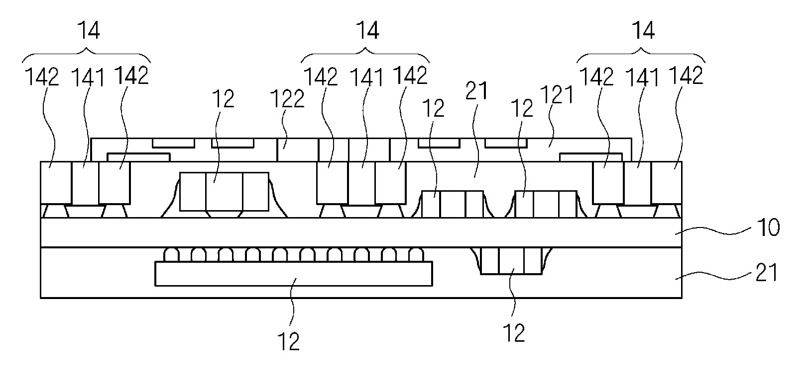
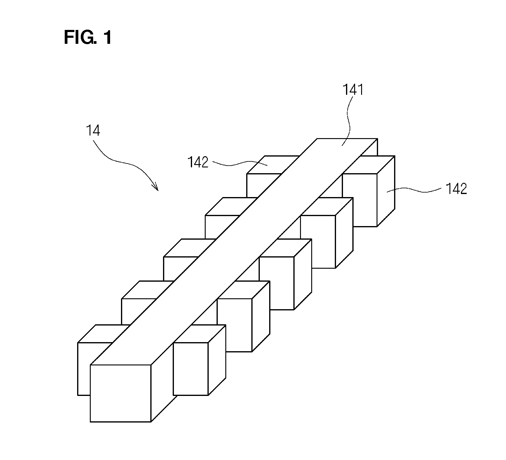
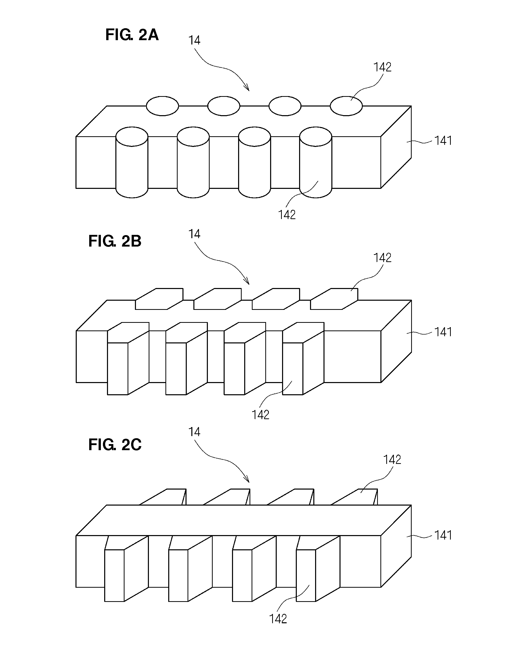
[0072]FIG. 1 is a perspective view that illustrates a configuration of a terminal connection substrate arranged in a module substrate according to a first preferred embodiment of the present invention. A terminal connection substrate 14 according to the first preferred embodiment of the present invention includes an insulator 141 made of a ceramic, a glass, an epoxy resin, or the like and a plurality of columnar terminal electrodes 142 arranged in a line on each of both lateral surfaces of the insulator 141.

[0073]Each of the terminal electrodes 142 when the terminal connection substrate 14 is mounted on a base substrate may be preferably higher than an electronic component (SMD) mounted on the base substrate. When the terminal electrode 142 has the shape of a rectangular prism, as illustrated in FIG. 1, the rectangular prism shape having an aspect ratio of the height and width of the terminal electrode 142 (=height / width) of substantially one can prevent deformation of the terminal ...

second preferred embodiment

[0093]A configuration of the terminal connection substrate arranged in the module substrate according to a second preferred embodiment of the present invention preferably is substantially the same as that in the first preferred embodiment, and thus the same reference numerals are used and the detailed description is not repeated here. The module substrate according to the second preferred embodiment of the present invention differs from that in the first preferred embodiment in that, after the plurality of electronic components 12 and the plurality of terminal connection substrates 14 are mounted on the base substrate 10, the plurality of mounted electronic components 12 and terminal connection substrates 14 are sealed with resin, and the top surface of the sealing resin is ground.

[0094]FIGS. 7A-7C include cross-sectional views that illustrate steps of manufacturing the module substrate according to the second preferred embodiment of the present invention in a plane orthogonal to th...

third preferred embodiment

[0106]FIGS. 11A-11D include perspective views that illustrate steps of manufacturing the module substrate according to a third preferred embodiment of the present invention. First, as illustrated in FIG. 11A, solder is printed on desired surface electrodes out of the surface electrodes of a composite substrate 1 from which a plurality of module substrates (base substrates 10) can be cut. The composite substrate 1 can be a low temperature co-fired ceramics (LTCC) substrate, an organic substrate, or the like and is not particularly limited.

[0107]In producing the module substrate using an LTCC substrate, ceramic slurry coating is first applied on a PET film, it is then dried, and a ceramic green sheet having a thickness of about 10 μm to about 200 μm, for example, is produced. Via holes each having a diameter of approximately 0.1 mm are formed in the produced ceramic green sheet from the PET film side using a mold, a laser, or the like.

[0108]Next, electrode paste in which metal powder ...


PUM

PropertyMeasurementUnit
Compositionaaaaaaaaaa
Shapeaaaaaaaaaa
Electrical conductoraaaaaaaaaa

Abstract

In a module substrate, a plurality of terminal connection substrates each including an insulator and a plurality of columnar terminal electrodes arranged on a single lateral surface or both lateral surfaces of the insulator is mounted on a single side of a composite substrate such that at least one of the terminal connection substrates extends over a border between a plurality of neighboring module substrates. The composite substrate, in which the plurality of terminal connection substrates is mounted on the single side and a plurality of electronic components is mounted on at least the single side, is divided at a location where the module substrates are to be cut from the composite substrate.

Description

BACKGROUND OF THE INVENTION[0001]1. Field of the Invention[0002]The present invention relates to a module substrate obtained by dividing a composite substrate including a plurality of electronic components mounted on a single side or both sides thereof and cutting the module substrates from the composite substrate, a module-substrate manufacturing method of cutting a plurality of module substrates from a composite substrate, and a terminal connection substrate.[0003]2. Description of the Related Art[0004]With size and weight reduction of an electronic device in recent years, a module substrate mounted on the electronic device itself also needs to reduce its size and weight. Therefore, electronic components are mounted on both sides of the module substrate using a lead terminal, a solder ball, a cavity structure, or the like to reduce the size and weight.[0005]Japanese Patent No. 3960479 discloses a method of manufacturing a semiconductor apparatus having an inexpensive double-sided ...

Claims


Application Information

Patent Timeline
IPC IPC(8): H05K7/06H05K3/30H05K1/00
CPCH01L21/561H01L23/3107H01L23/49805H01L23/49833H01L24/16H01L24/97H01L25/0655H01L2224/97H01L2924/01004H01L2924/01013H01L2924/01029H01L2924/01047H01L2924/01078H01L2924/01079H01L2924/01082H01L2924/09701H01L2924/15313H01L2924/19105H01L2924/19106H05K1/186H05K3/0052H05K3/4007H01L2224/81H01L25/165H01L2224/16227H01L2924/01005H01L2924/01006H01L2924/01033H01L2924/014H01L2224/45147H01L2924/00H01L23/49811H01L2224/16225H01L2924/00014H01L2224/48H01L2224/16H01L2924/181Y10T29/4913H01L2924/12042H01L2924/00012H01L2924/00011H01L2224/0401
Inventor YAMAMOTO, ISSEI
Owner MURATA MFG CO LTD
Why Eureka
Try Eureka