Photovoltaic device and method of its fabrication

a photovoltaic and photovoltaic technology, applied in the direction of semiconductor/solid-state device manufacturing, semiconductor/solid-state device manufacturing, electrical apparatus, etc., can solve the problems of increasing cell series resistance, increasing resistive power loss, and reducing resistive power loss at the expense of larger shading loss

Inactive Publication Date: 2013-01-03
SHENKAR COLLEGE OF ENG & DESIGN +1
View PDF9 Cites 35 Cited by
  • Summary
  • Abstract
  • Description
  • Claims
  • Application Information

AI Technical Summary

Problems solved by technology

On the one hand, increasing the spacing between the metal lines (metal conductors), in order to reduce the shading, results in an increase in the cell series resistance with the direct outcome of increased resistive power loss.
On the other hand, decrease of the spacing between the metal lines results in lower resistive power loss at the expense of larger shading loss.
However, this solution has certain drawbacks.
The short wavelength photo generated electrons close to the top surface of the cell have to diffuse to the bottom side of the p-substrate through the few hundred microns of the wafer thickness with the pe...

Method used


Image

  • Photovoltaic device and method of its fabrication
  • Photovoltaic device and method of its fabrication
  • Photovoltaic device and method of its fabrication

Examples


Embodiment Construction

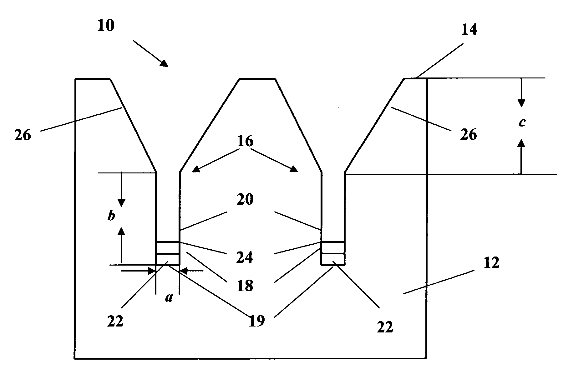
[0036]Referring to FIG. 1, there is schematically illustrated a cross sectional view of a photovoltaic device, generally designated 10, according to an embodiment of the invention. The device 10 includes one or more photovoltaic cells electrically connected in series. The cell(s) is / are fabricated in a semiconductor substrate (wafer) 12, typically silicon p-type substrate. The substrate 12 has a patterned surface 14, the pattern comprising an array of spaced-apart grooves 16. The groove 16 has a bottom portion 18 configured as a deep narrow cavity having a bottom surface 19 and side walls 20 substantially perpendicular to the surface 14 of the structure 10.

[0037]Such arrangement of the side walls 20 substantially perpendicular to the surface 14, or the so-called “substantially vertical” bottom portion 18 can be obtained by making the side walls 20 parallel to each other or arranged with a small angle between them. In the latter case, the configuration is such that a distance between...


PUM


Abstract

A photovoltaic device is presented including one or more cell units. The photovoltaic device comprises a semiconductor substrate having a patterned light collecting surface defining an array of spaced-apart substantially parallel first grooves. Each of these first grooves has a bottom portion, comprising a bottom surface and side walls extending from the bottom portion and being substantially perpendicular to the surface of the device. A heavily doped semiconductor layer in the form of spaced-apart regions is located at the bottom surfaces of the first grooves respectively. Further improvement of performance is obtained by deposition of thin metal lines on top of the heavily doped spaced apart lines.

Description

FIELD OF THE INVENTION[0001]This invention relates to a photovoltaic device and a method of its manufacture.BACKGROUND OF THE INVENTION[0002]Photovoltaic devices are formed by an array of photovoltaic cells fabricated in semiconductor wafers with appropriate electrical connection between them forming a readout circuit that collects photocurrent generated by multiple cells of the same cell unit (array). The readout circuit includes metal conductors from which the electric current is further transferred via so-called bus lines. A major factor in the performance of a photovoltaic device is the shading of the active area of the cell unit (i.e. its light collection surface) by the metal conductors and the bus lines, which all extend on top of the light collecting surface. The larger the surface area covered by the metal lines (metal conductors), the smaller the active, light collection area of the device. On the one hand, increasing the spacing between the metal lines (metal conductors),...

Claims


Application Information

Patent Timeline
IPC IPC(8): H01L31/0224H01L31/18H01L31/0236
CPCH01L31/022425H01L31/022433Y02E10/547H01L31/068H01L31/0236H01L31/02363
Inventor SHAPPIR, JOSEPH
Owner SHENKAR COLLEGE OF ENG & DESIGN
Why Eureka
Try Eureka