

Laminate and manufacturing method for same
- Summary
- Abstract
- Description
- Claims
- Application Information
AI Technical Summary
Benefits of technology
Problems solved by technology
Method used
Image

Examples
embodiment 1
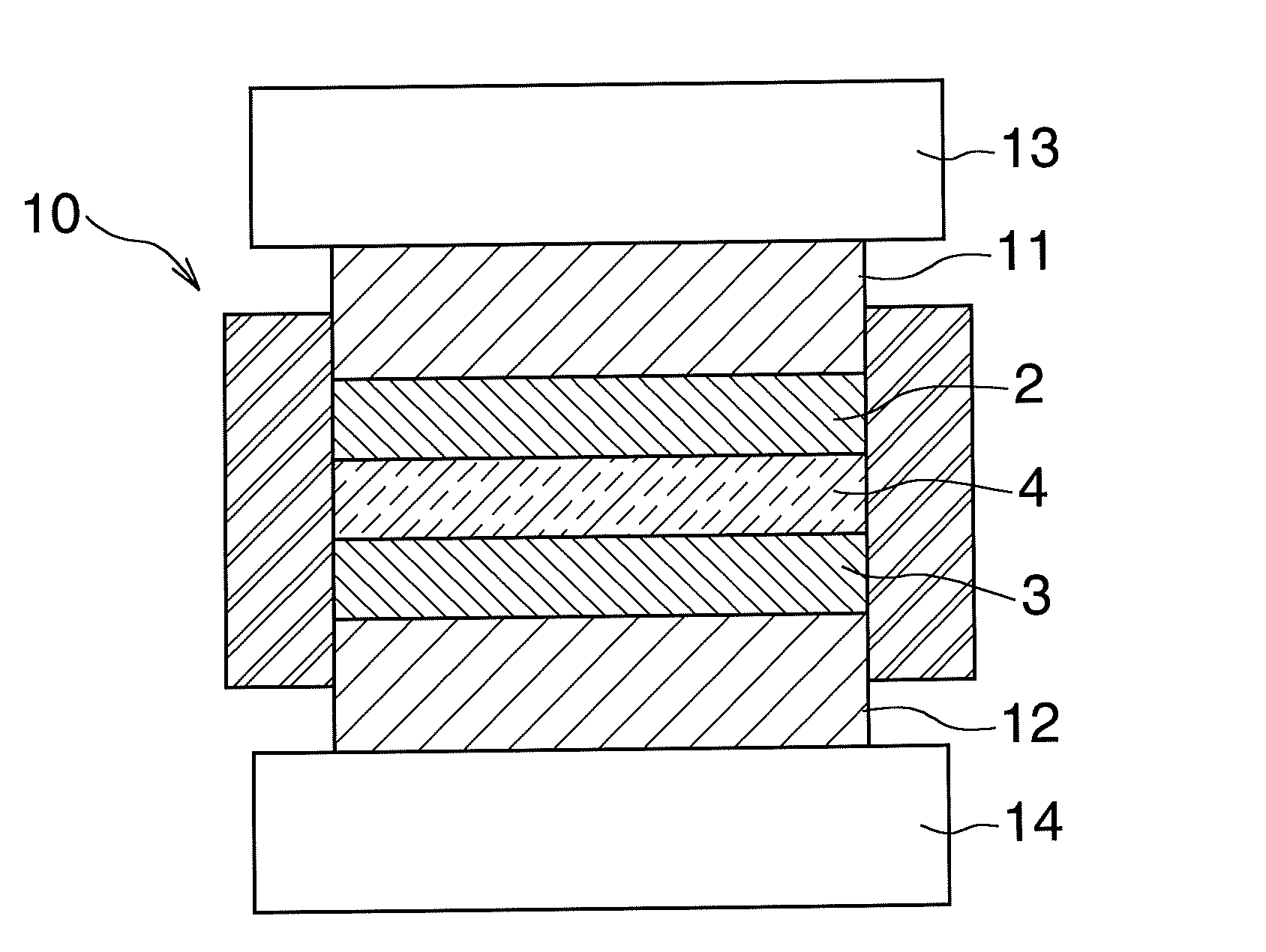
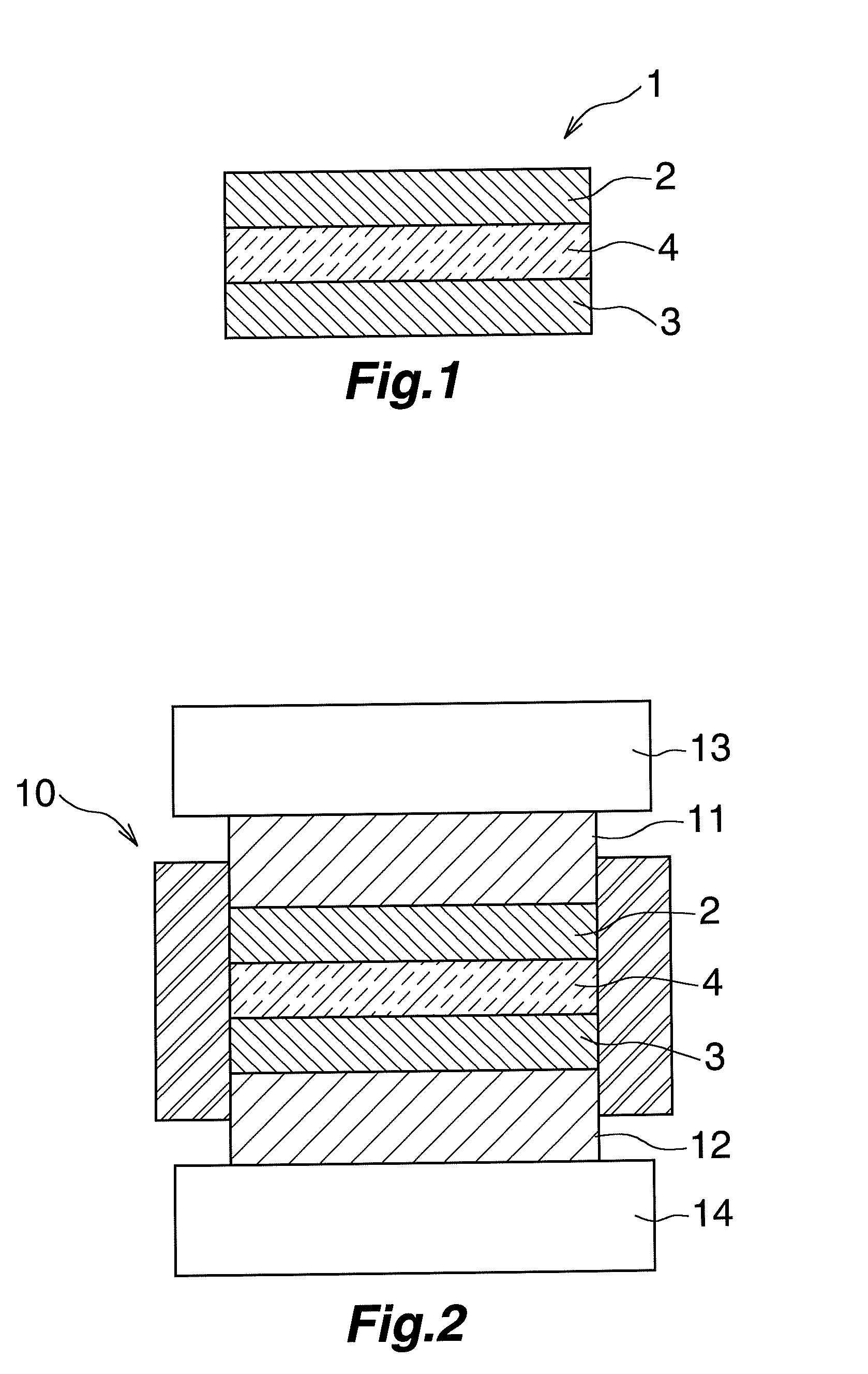
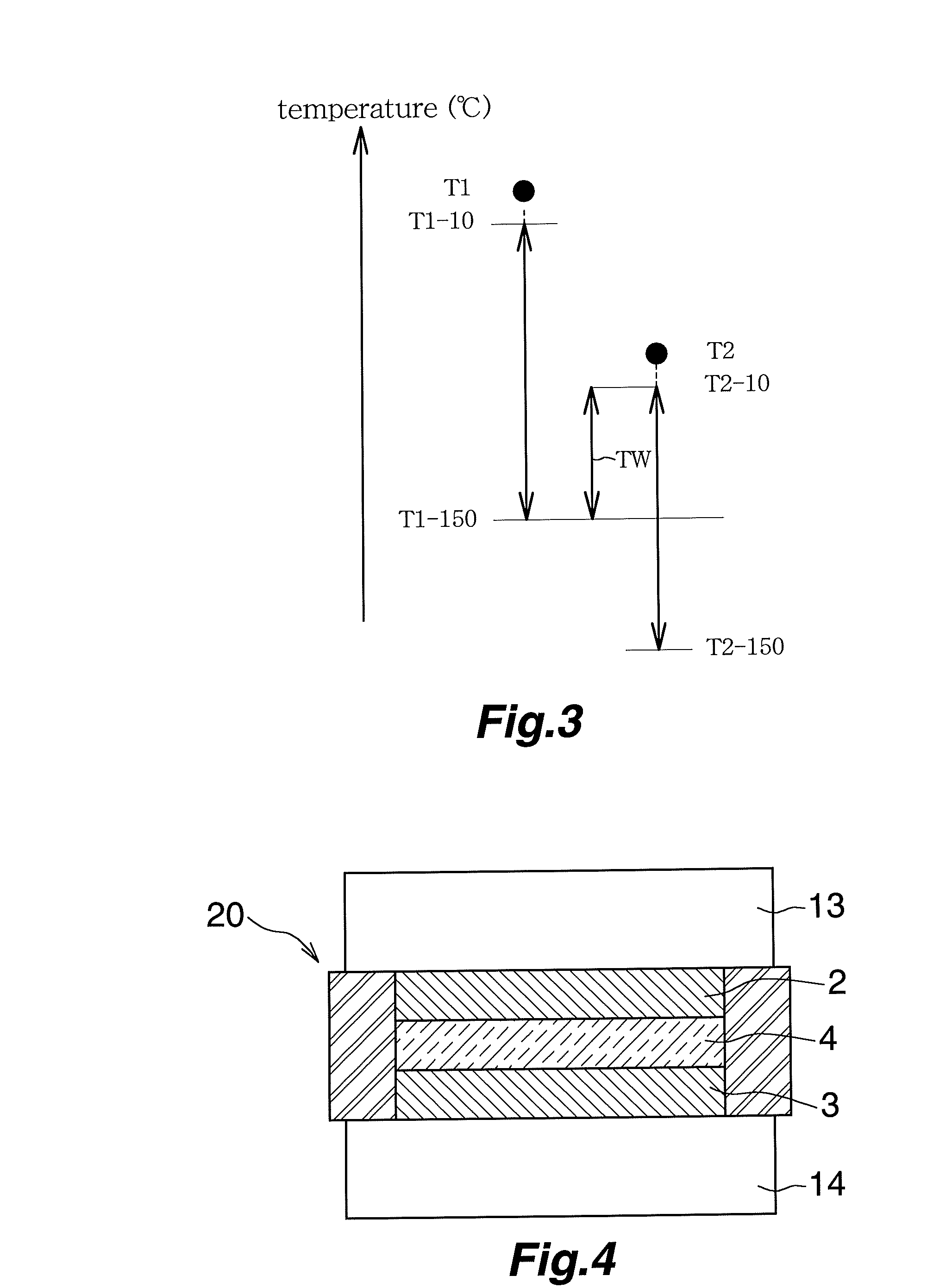
[0068]This embodiment is shown in FIGS. 1 to 3. FIG. 1 shows a layered material according to Embodiment 1 of the present invention, and FIG. 2 shows a method for producing the layered material of FIG. 1. FIG. 3 shows temperature ranges of heating upon practice of the method of FIG. 2.
[0069]As shown in FIG. 1, the layered material (1) includes a plurality of metal sheets (2) and (3) and at least one ceramic sheet (4), wherein the metal sheets (2) and (3) and the ceramic sheet (4) are stacked together such that the ceramic sheet (4) is adjacent to each of the metal sheets (2) and (3), and the ceramic sheet (4) is bonded to the adjacent metal sheets (2) and (3) through spark plasma sintering. In the layered material (1), the two (upper and lower) metal sheets (2) and (3) and the one ceramic sheet (4) are stacked together such that the ceramic sheet (4) is disposed between the metal sheets (2) and (3), and the metal sheets (2) and (3) are bonded to the ceramic sheet (4) through spark pl...
embodiment 2
[0092]This embodiment is shown in FIGS. 8 and 9. FIG. 8 shows a layered material according to Embodiment 2 of the present invention, and FIG. 9 shows a method for producing the layered material of FIG. 8.
[0093]As shown in FIG. 8, the layered material (30) is a modification of the layered material (1) according to Embodiment 1, wherein a metal sheet (31) made of a material which does not melt at the heating temperature during spark plasma sintering for producing the layered material (30) is stacked and bonded, through spark plasma sintering, to the surface of at least one of the upper and lower metal sheets (2) and (3) on the side opposite the surface bonded to the ceramic sheet (4) (in this case, to the bottom surface of the lower metal sheet (3)). Specifically, when the metal sheets (2) and (3) have the same melting temperature, the metal sheet (31) is formed of a material having a melting temperature higher than that of the metal sheets (2) and (3), whereas when the metal sheets (...
embodiment 3
[0105]This embodiment is shown in FIG. 10. FIG. 10 shows a layered material according to Embodiment 3 of the present invention.
[0106]As shown in FIG. 10, the layered material (35) is a modification of the layered material (1) according to Embodiment 1, wherein a high-melting-temperature metal sheet (36) made of a material which does not melt at the heating temperature during spark plasma sintering for producing the layered material (35) is stacked and bonded, through spark plasma sintering, to the surface of at least one of the upper and lower metal sheets (2) and (3) on the side opposite the surface bonded to the ceramic sheet (4) (in this case, to the top surface of the upper metal sheet (2)).
[0107]The metal sheets (2) and (3) are formed of Al or an Al alloy, and the high-melting-temperature metal sheet (36) is formed of one material selected from the group consisting of Cu, Ag, Au, Ni, a Cu alloy, an Ag alloy, an Au alloy, and an Ni alloy. Such a material exhibits high thermal co...
PUM
| Property | Measurement | Unit |
|---|---|---|
| Temperature | aaaaa | aaaaa |
| Temperature | aaaaa | aaaaa |
| Pressure | aaaaa | aaaaa |
Abstract
Description
Claims
Application Information