Electronic device and method for manufacturing same

Active Publication Date: 2013-01-10
ASAHI GLASS CO LTD
View PDF2 Cites 31 Cited by
  • Summary
  • Abstract
  • Description
  • Claims
  • Application Information

AI Technical Summary

Benefits of technology

[0015]In accordance with the electronic device and the processes for producing the same of the present invention, it is possible to improve the bonding strength between glass substrates and a sealing laye

Problems solved by technology

Since the sealing temperature of the sealing glass is at a level of 400 to 600° C., properties of the electronic element portion of the OEL element or the like will be deteriorated when firing is conducted by using a heating furnace.
The generation of residue stress at the bonding interfaces causes cracks or fractures in the boding portion or the glass substrates, or a decrease in the bonding strength between the glass substrates and the bonding layer.
When the local heating and sealing operation, s

Method used


Image

  • Electronic device and method for manufacturing same
  • Electronic device and method for manufacturing same
  • Electronic device and method for manufacturing same

Examples


example 1

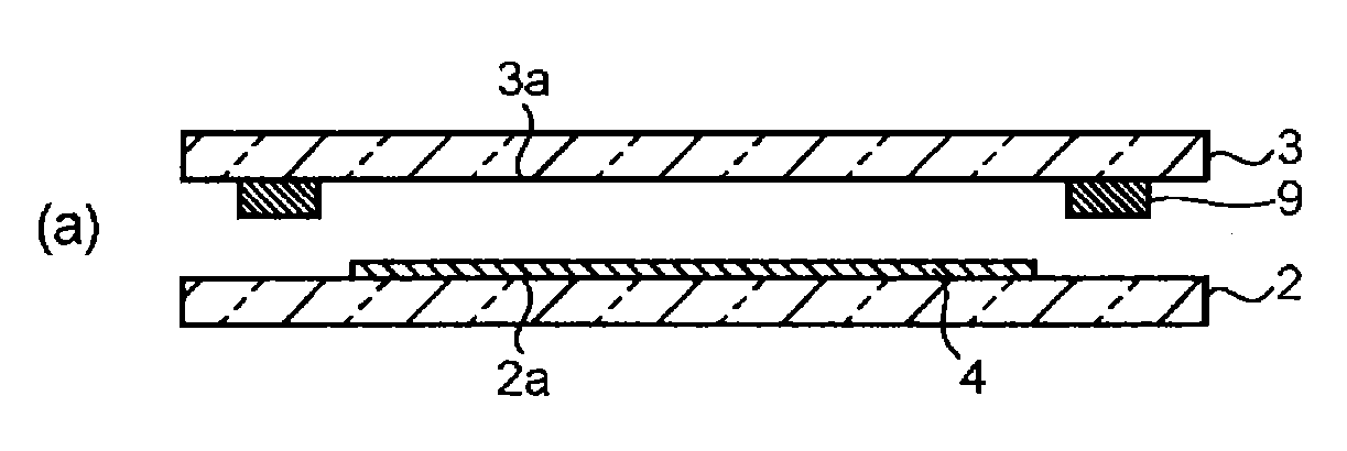
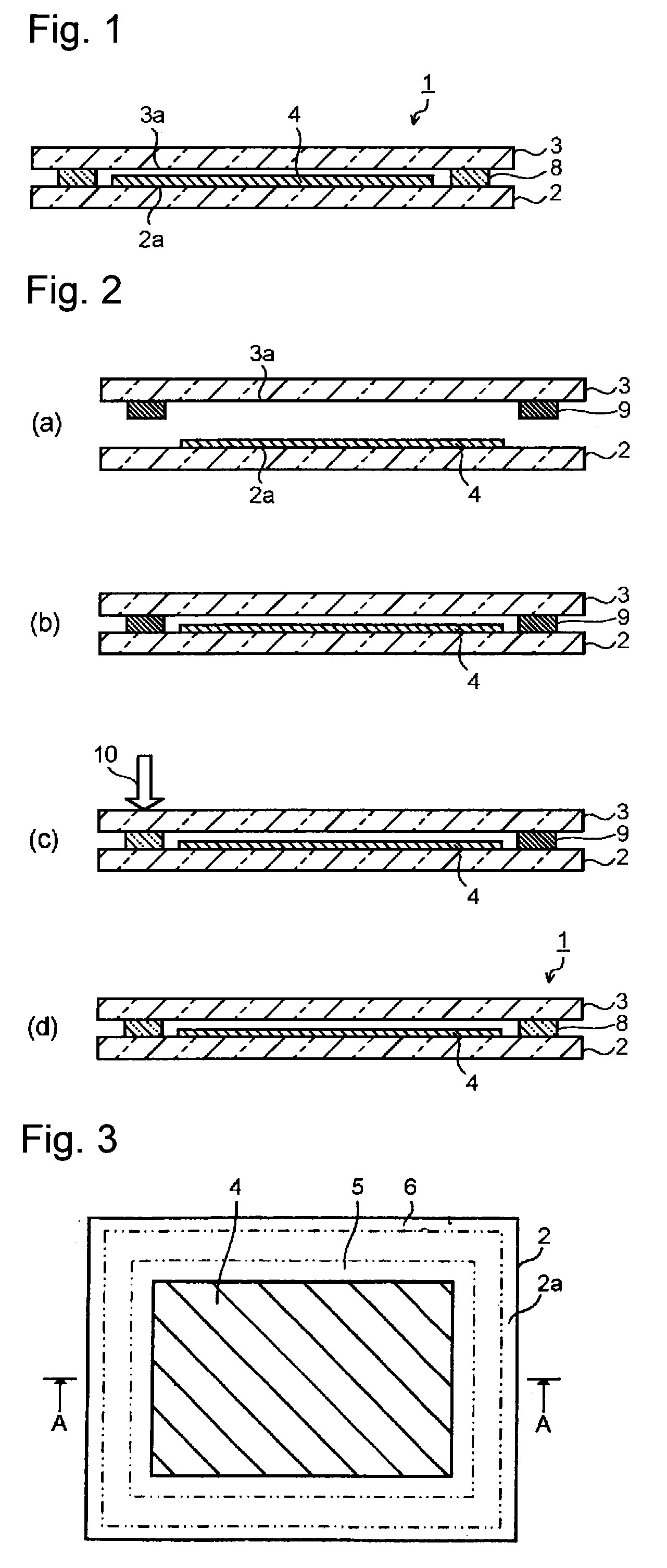
[0076]First, a bismuth glass frit (softening point: 420° C.) having a composition including 83% of Bi2O3, 5.5% of B2O3, 11% of ZnO and 0.5% of Al2O3 by mass proportion, and further including 12 ppm of Na2O by mass proportion, cordierite powder as a low-expansion filler, and a laser absorbent, as an electromagnetic wave absorption material, having a composition including 24% of Fe2O3, 22% of CuO, 20% of Al2O3 and 34% of MnO by mass proportion were prepared. The content of Na2O was analyzed by ICP. Although the total amount of the main components is represented as 100 mass % with regard to the composition ratio of the bismuth glass frit for descriptive purposes, the amount of Na2O as a minor component is contained in the total of the components of the sealing glass (100 mass %).

[0077]68 vol % of the bismuth glass frit, 25 vol % of the cordierite powder and 7 vol % of the laser absorbent were mixed to prepare a sealing material (thermal expansion coefficient: 71×10−7 / ° C.). By mixing 8...

example 2

[0080]The formation of a sealing material layer and the sealing of a first glass substrate and a second glass substrate by use of laser light were carried out in the same manner as in Example 1 except that a bismuth glass frit containing 100 ppm of Na2O by mass proportion (softening point: 420° C.) was used. The sealing material layer had a temperature of 650° C. during irradiation of the laser light as in Example 1. An electronic device having the glass panel thus fabricated was subjected to the property evaluation described later.

example 3

[0081]The formation of a sealing material layer and the sealing of a first glass substrate and a second glass substrate by use of laser light were carried out in the same manner as in Example 2 except that the laser light had an output of 28 W (output density: 1,393 W / cm2). The sealing material layer had a temperature of 730° C. during irradiation of the laser light. This heating temperature corresponds to (T+310° C.). An electronic device having the glass panel thus fabricated was subjected to the property evaluation described later.


PUM

PropertyMeasurementUnit
Fractionaaaaaaaaaa
Percent by volumeaaaaaaaaaa

Abstract

When local heating by use of laser sealing or the like is applied, the bonding strength between glass substrates and a sealing layer is improved to provide an electronic device having increased reliability. An electronic device includes a first glass substrate, a second glass substrate, and a sealing layer to seal an electronic element portion disposed between these glass substrates. The sealing layer is a layer obtained by locally heating a sealing material by an electromagnetic wave, such as laser light or infrared light, to melt-bond the sealing material, the sealing material containing sealing glass, a low-expansion filler and an electromagnetic wave absorber. In the first and second glass substrates, each reacted layer is produced to have a maximum depth of at least 30 nm from an interface with the sealing layer.

Description

TECHNICAL FIELD[0001]The present invention relates to an electronic device and a process for producing the same.BACKGROUND ART[0002]A flat panel display device (FPD), such as an organic EL (electroluminescence) display (OELD), a plasma display panel (PDP) or a liquid crystal display device (LCD), has such a structure that a glass substrate for an element having a light-emitting element formed and a glass substrate for sealing are disposed to face each other and the light-emitting element or the like is sealed in a glass package comprising two such glass substrates bonded. Further, for a solar cell, such as a dye-sensitized solar cell, application of a glass package having a solar cell element (dye-sensitized photoelectric conversion element) sealed with two glass substrates has been studied.[0003]As a sealing material to seal a space between two glass substrates, a sealing resin or sealing glass has been used. Since an organic EL (OEL) element or the like is likely to undergo deteri...

Claims


Application Information

Patent Timeline
IPC IPC(8): C03B23/20H05B33/10H05B33/04B32B7/04G02F1/1339
CPCG02F1/1339Y10T428/239H01J9/26H01J2211/446H01J2211/48H01L51/448H01L51/524H01L51/5246Y02E10/542H01G9/2077Y02E10/549C03C3/14C03C8/04C03C8/18C03C8/24C03C23/0025G02F2202/28Y02P70/50H10K30/88H10K50/841H10K50/8426
Inventor KAWANAMI, SOHEIAMI, YOSHINORIMITSUI, YOKO
Owner ASAHI GLASS CO LTD
Why Eureka
Try Eureka