Method of processing optical device wafer

a technology of optical devices and wafers, applied in the direction of solid-state devices, semiconductor/solid-state device details, manufacturing tools, etc., can solve the problem of difficult to accurately position the condensing point of laser beams to the buffer layer

a technology of optical devices and wafers, applied in the direction of solid-state devices, semiconductor/solid-state device details, manufacturing tools, etc., can solve the problem of difficult to accurately position the condensing point of laser beams to the buffer layer

US20130017640A1Inactive Publication Date: 2013-01-17DISCO CORP

Image

  • Method of processing optical device wafer
  • Method of processing optical device wafer
  • Method of processing optical device wafer

Examples


Embodiment Construction

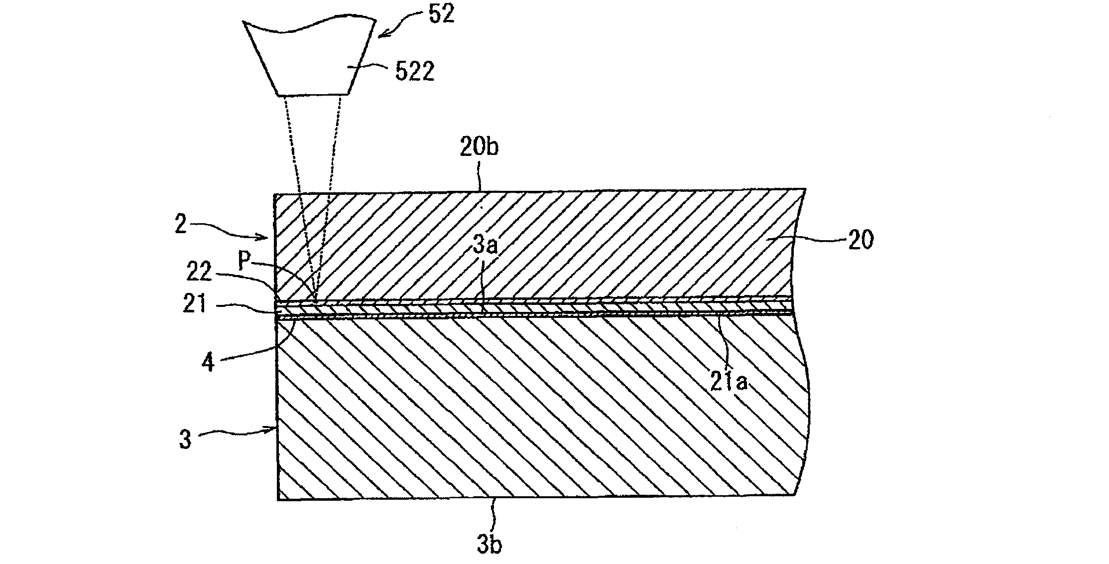
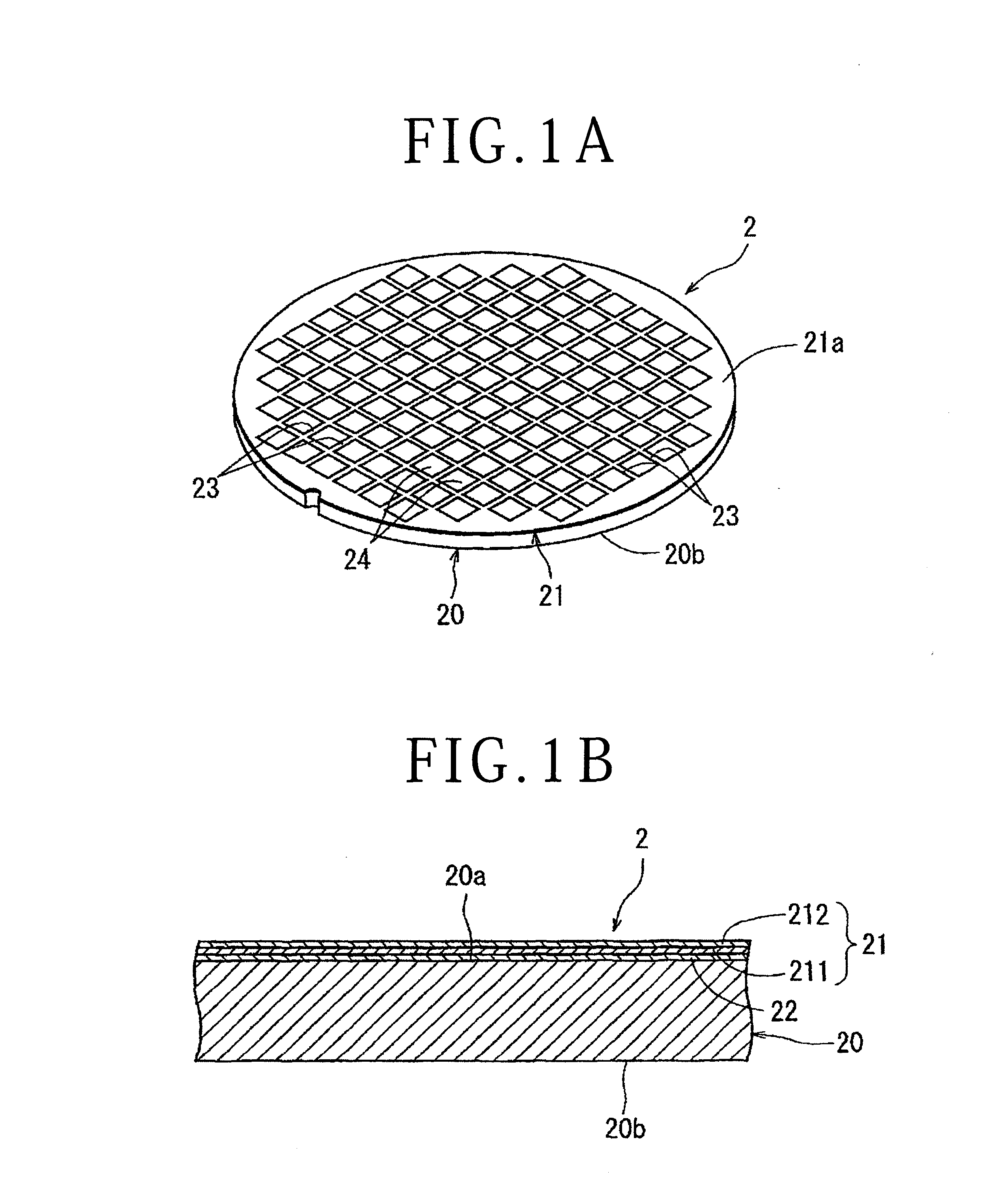
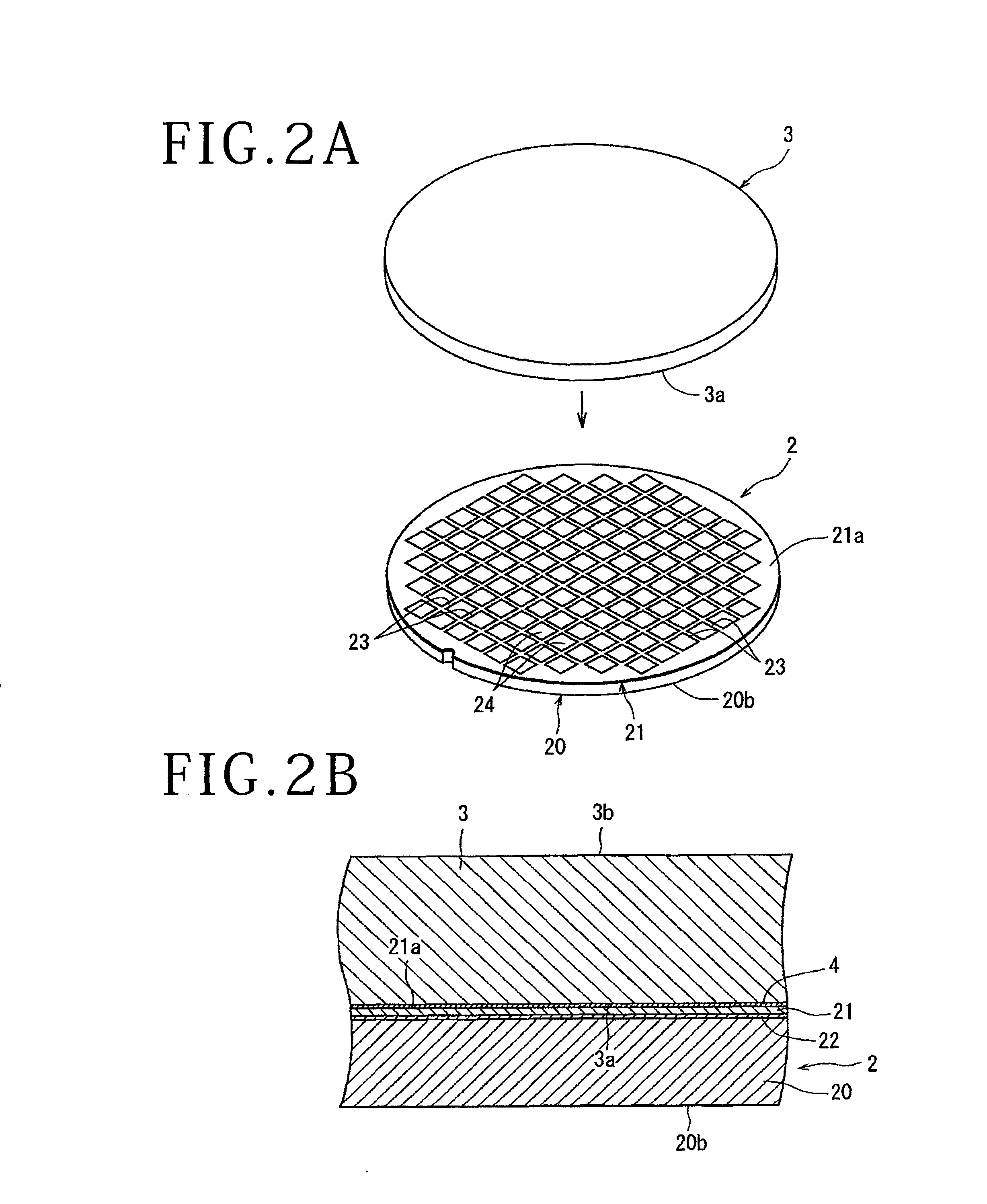
[0021]Now, preferred embodiments of the method of processing an optical device wafer according to the present invention will be described in detail below, referring to the attached drawings. FIGS. 1A and 1B show a perspective view of an optical device wafer to be processed by the method of processing an optical device wafer according to the present invention and a sectional view showing, in an enlarged form, an essential part of the optical device wafer. The optical device wafer 2 shown in FIG. 1A has a structure in which an optical device layer 21 composed of an n-type gallium nitride semiconductor layer 211 and a p-type gallium nitride semiconductor layer 212 is formed, by epitaxial growth process, over a surface 20a of a substantially circular disc-shaped sapphire substrate 20. Incidentally, in stacking the optical device layer 21 composed of the n-type gallium nitride semiconductor layer 211 and the p-type gallium nitride semiconductor layer 212 over the surface of the sapphire ...


PUM

PropertyMeasurementUnit
Lengthaaaaaaaaaa
Timeaaaaaaaaaa
Timeaaaaaaaaaa

Abstract

A method of processing an optical device wafer having an optical device layer including an n-type semiconductor layer and a p-type semiconductor layer stacked over a sapphire substrate, a buffer layer therebetween, allowing peeling of the sapphire substrate. The method includes joining a transfer substrate to the optical device layer, breaking the buffer layer by irradiation with a pulsed laser beam from the sapphire substrate side of the wafer with the transfer substrate joined to the optical device layer, and peeling the sapphire substrate from the optical device wafer with the buffer layer broken, transferring the optical device layer onto the transfer substrate. The pulsed laser beam has a wavelength longer than an absorption edge of the sapphire substrate and shorter than an absorption edge of the buffer layer, and a pulse width set so that a thermal diffusion length will be not more than 200 nm.

Description

BACKGROUND OF THE INVENTION[0001]1. Field of the Invention[0002]The present invention relates to a method of processing an optical device wafer in which an optical device layer including an n-type gallium nitride semiconductor layer and a p-type gallium nitride semiconductor layer or the like is stacked over a surface of a sapphire substrate, with a buffer layer therebetween, so as to peel the sapphire substrate from the optical device wafer.[0003]2. Description of the Related Art[0004]In an optical device manufacturing process, an optical device wafer is configured by forming optical devices such as light emitting diodes, laser diodes, etc. in a plurality of regions demarcated by a plurality of streets formed in a grid pattern on an optical device layer which includes an n-type semiconductor layer and a p-type semiconductor layer and which is stacked over a surface of a substantially circular disc-shaped sapphire substrate, with a buffer layer therebetween. Subsequently, the optica...

Claims


Application Information

Patent Timeline
17 Jan 2013
Publication
US20130017640A1
IPC
H01L33/32; B23K26/00; B23K26/40; H01L21/304
CPC
B23K26/00; H01L33/0095; H01L23/00; B23K26/40; H01L2924/0002; H01L2924/00; H01L21/78; H01L21/30
Inventors
MORIKAZU, HIROSHI; NISHINO, YOKO