Lighting devices with prescribed colour emission

a technology of colour emission and light source, applied in the field of optical devices, can solve the problems of inability to generate white light using a conventional led, difficulty in converting layers based on qds, and difficulty in generating white light, so as to avoid losses and deficiencies, improve the emission spectrum, and minimize energy loss.

Active Publication Date: 2013-01-31
YISSUM RES DEV CO OF THE HEBREWUNIVERSITY OF JERUSALEM LTD
View PDF0 Cites 29 Cited by
  • Summary
  • Abstract
  • Description
  • Claims
  • Application Information

AI Technical Summary

Benefits of technology

[0022]3): FRET avoidance or minimalization. In a regular QD conversion layer, The typical length scale of FRET is ˜10 nm, with 1 / R6 dependence, where R is the distance between two QD particles. For example, if the initial emission QY is 0.8, the QY is reduced to 0.64 after a single FRET process. FRET also leads to red shift, which is avoided in a SNP layer. A densely-packed SNP conversion layer (with small distances between the SNPs, e.g. 0-50 nm) owing to their unique characteristics will avoid the losses and deficiencies related to FRET commonly encountered in densely-packed QD layers. Exemplarily, “densely-packed” as applied to SNPs in conversion layers of the invention may include ˜85% SNPs and ˜15% ligands dispersed in a host matrix.
[0023]In an embodiment, a SNP layer may be coated on an optical device such as a LED to improve its emission spectrum. In another embodiment, a separate SNP layer may be positioned in the optical path of light emitted by one or more LEDs for the same purpose. In yet another embodiment, a layered SNP structure comprising a plurality of different SNP conversion sub-layers may be coated on a LED. In yet another embodiment, the layered SNP structure may be positioned in the optical path of light emitted by LEDs. In some embodiments, a SNP layer may be spaced apart from a LED by a coupling layer which may be an air gap, an optical filter such as short wavelength (UV, blue) pass filter, a long wavelength (e.g. green or red) reflection filter, or an index matching layer which minimizes energy loss by reflection. The spacing between the LED and the SNP layer can for example be used to minimize heating due to heat flow from the LED to the SNP layer.

Problems solved by technology

However, “white” light, which is required for a very large portion of the lighting industry, cannot be generated using a conventional LED.
However, such white light is almost always non-ideal and has in many cases undesired or unpleasant characteristics which may require improvement or correction.
However, conversion layers based on QDs have challenges.
This undesired process leads to reduced energy efficiency of a regular QD conversion layer and also to changes in the colour composition.
In devices where phosphor is used as part of a light conversion scheme to produce green light, the QD layers will absorb partially the light from the phosphor as well, leading to both re-absorption losses and colour changes.
The efficiency of the FRET process is very sensitive to distance.
FRET leads to colour change (red shift) and losses in the efficiency of light conversion.

Method used


Image

  • Lighting devices with prescribed colour emission
  • Lighting devices with prescribed colour emission
  • Lighting devices with prescribed colour emission

Examples


example 2

Lighting Device with Diffusive RSNP Conversion Layer Within Polymer Host Providing Combination of Blue and Red Light

[0071]A diffusive RSNP layer was prepared using the procedure in Example 1, with a modification that 1.3 mg of RSNP was dissolved in 1 ml Toluene and that after the 10 minutes stirring of RSNPs in polymer, 5 mg of BaSO4 particles were added to the solution and stirred for another 15 minutes. The resulting film had diffusive properties that enhanced the optical emission and increased the extraction of the light in a required direction.

[0072]The RSNP layer was incorporated in a lighting device as shown in FIG. 5B. A blue LED emitting at 455 nm was used to illuminate the RSNP layer. The lighting output was measured and the light spectrum is presented in FIG. 12A, which shows a combination of a blue remnant from the blue LED and a red component from the RSNP conversion layer.

example 3

Lighting Device with RSNP Conversion Layer Within Silicone RTV Providing Combination of Blue and Red Light

[0073]A RSNP layer in Silicone RTV was prepared as follows: 1 g of RTV615A (Momentive, 22 Corporate Woods Boulevard, Albany, N.Y. 12211 USA) was stirred with 0.1 g of RTV615B for 10 min. 1.5 mg of CdSe / CdS RSNPs with overall dimensions of 27×5.5 nm emitting at 635 nm was dissolved in 250 μl Toluene. The RSNP solution was added to the silicone mixture while stiffing, then vacuumed until no bubbles remained. The solution was then deposited on a glass substrate and sandwiched using another glass substrate. 600 μm-thick spacers were positioned between the two glass substrates to obtain the desired film thickness. The sandwiched structure was then placed on a hot plate at 150° C. for 15 minutes, after which the solution became solid. The measured film thickness was 600 μm.

[0074]The RSNP layer was incorporated in a lighting device as shown in FIG. 5B. A blue LED emitting at 455 nm was...

example 4

Lighting Device with Thin Dense Spin-Coated RSNP Conversion Layer Providing Red Light

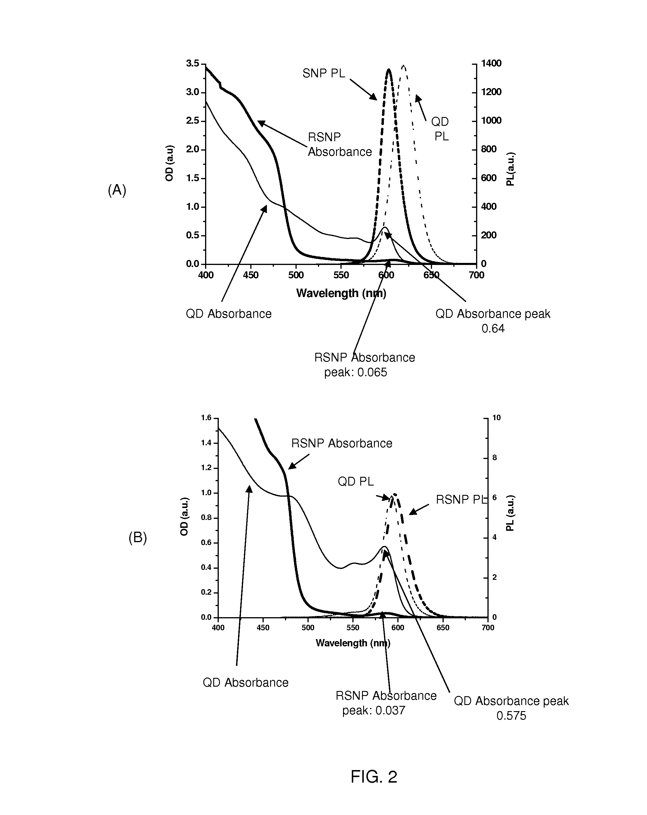
[0075]A dense RSNP layer was prepared as follows: first prepared was a solution of 35×5.4 nm CdSe / CdS RSNPs, emitting at 635 nm, in Toluene with 1:4 weight / volume (mg / μL) ratio. 20 μL of the solution was drop cast on a soda lime glass substrate and spread by spin coating at 2000 rpm. The deposited film was measured to have an absorbance OD of 0.51 at 455 nm, and OD of 0.9 at 360 nm. The thickness was 0.510 um as measured by a profilometer. FIG. 13A shows the absorption (dotted line) and the PL (full line) spectra of this RSNP layer. The emission maximum is at 633 nm, with a FWHM of 33 nm. The absorption OD is 0.96 at 360 nm, 0.5 at 455 nm, 0.035 at 540 nm and 0.025 at 600-750 nm, the latter 20 times smaller than the OD at 455 nm.

[0076]The RSNP layer was incorporated in a lighting device as shown in FIG. 5A A UV LED at 360 nm was used to illuminate the RSNP layer, and provided light output in the red...


PUM

PropertyMeasurementUnit
central emission wavelengthaaaaaaaaaa

Abstract

Optical conversion layers based on semiconductor nanoparticles for use in lighting devices, and lighting devices including same. In various embodiments, spherical core/shell seeded nanoparticles (SNPs) or nanorod seeded nanoparticles (RSNPs) are used to form conversion layers with superior combinations of high optical density (OD), low re-absorbance and small FRET. In some embodiments, the SNPs or RSNPs form conversion layers without a host matrix. In some embodiments, the SNPs or RSNPs are embedded in a host matrix such as polymers or silicone. The conversion layers can be made extremely thin, while exhibiting the superior combinations of optical properties. Lighting devices including SNP or RSNP-based conversion layers exhibit energetically efficient superior prescribed colour emission

Description

CROSS REFERENCE TO RELATED APPLICATIONS[0001]This application claims priority from U.S. Provisional Patent Applications No. 61 / 299,012 filed Jan. 28, 2010 and titled “Light source with prescribed colour emission” and 61 / 299,018 filed Jan. 28, 2010 and titled “Phosphor-nanoparticle combination”, both of which are incorporated herein by reference in its entirety.FIELD AND BACKGROUND[0002]Embodiments of the invention relate in general to optical devices which comprise semiconductor nanoparticles and in particular to lighting devices which include conversion layers having semiconductor quantum confined nanoparticles.[0003]Light emitting diodes (LED) offer significant advantages over incandescent and fluorescent lamps with respect to their high energy efficiency and long lifetimes. LEDs are applicable in diverse applications including displays, automobile and signage lighting and domestic and street lighting.[0004]A LED can emit monochromatic light in different regions of the spectrum, d...

Claims


Application Information

Patent Timeline
Patent Type & Authority Applications(United States)
IPC IPC(8): H01B1/06H01B1/10H01L33/50H01B1/00B82Y20/00B82Y30/00
CPCC09K11/02C09K11/565H01L33/505H01L33/502C09K11/883C09K11/7706C09K11/025C09K11/56Y10S977/774Y10S977/779Y10S977/95B82Y20/00
Inventor ARBELL, HAGAI
Owner YISSUM RES DEV CO OF THE HEBREWUNIVERSITY OF JERUSALEM LTD
Why Eureka
Try Eureka