Optical Device Structure Using GaN Substrates and Growth Structures for Laser Applications

a technology of optical devices and growth structures, applied in the direction of lasers, nanooptics, semiconductor lasers, etc., can solve the problems of less reliability than desired, the conventional edison light bulb disperses much thermal energy, and the drawbacks of the conventional edison light bulb, etc., to improve efficiency, cost, temperature sensitivity, and ruggedness

Active Publication Date: 2013-02-21
KYOCERA SLD LASER INC
View PDF3 Cites 121 Cited by
  • Summary
  • Abstract
  • Description
  • Claims
  • Application Information

AI Technical Summary

Benefits of technology

[0009]This invention provides a manufacturing method and a device for emitting electromagnetic radiation using semipolar or non-polar gallium containing substrates such as GaN, MN, InN, InGaN, AlGaN, and AlInGaN, and others. Merely by way of example the invention can be applied to the non-polar m-plane or to the semipolar (11-22), (30-31), (30-3-1), (20-21), (20-2-1), (30-32), or (30-3-2), or offcuts thereof. Merely by way of example, the invention can be applied to optical devices, lasers, light emit...

Problems solved by technology

Unfortunately, drawbacks exist with the conventional Edison light bulb.
First, the conventional light bulb dissipates much thermal energy.
Second, reliability is less than desired—the conventional light bulb routinely fails due to thermal expansion and contraction of the filament element.
They therefore are not ideal for applications requiring strong directionality or focus, such as projection displays, optical data storage, or specialized directed lighting.
The size, weight, and cost of the laser was undesirable as well.
As laser technology evolved, more efficient lamp pumped solid state laser designs were developed for the red and infrared wavelengths, but these technologies remained a challenge for blue and green lasers.
These had wall plug efficiency of ˜1%, and were more efficient than Ar-ion gas lasers, but were still too inefficient, large, expensive, and fragile for broad deployment outside of specialty scientific and medical applications.
Additionally, the ...

Method used


Image

  • Optical Device Structure Using GaN Substrates and Growth Structures for Laser Applications
  • Optical Device Structure Using GaN Substrates and Growth Structures for Laser Applications
  • Optical Device Structure Using GaN Substrates and Growth Structures for Laser Applications

Examples


Embodiment Construction

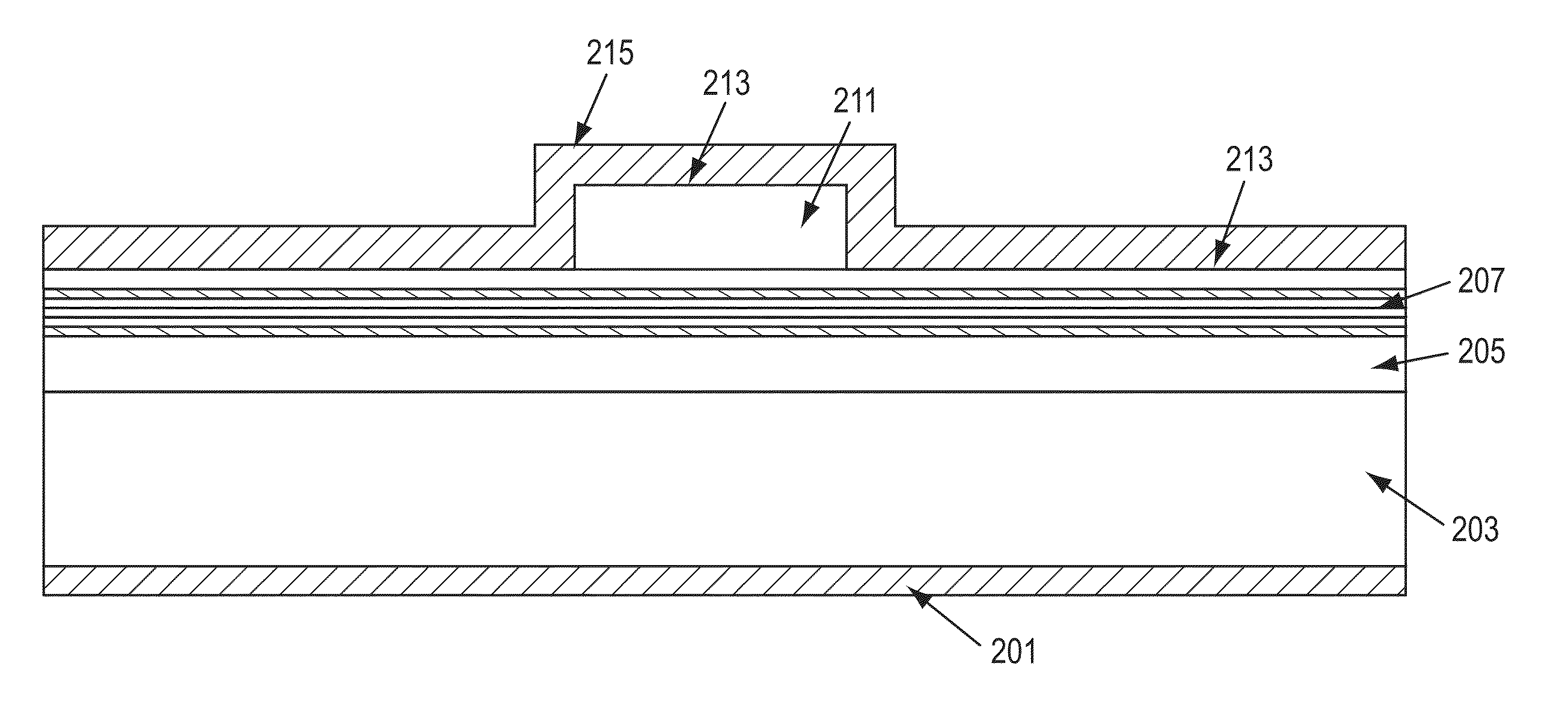
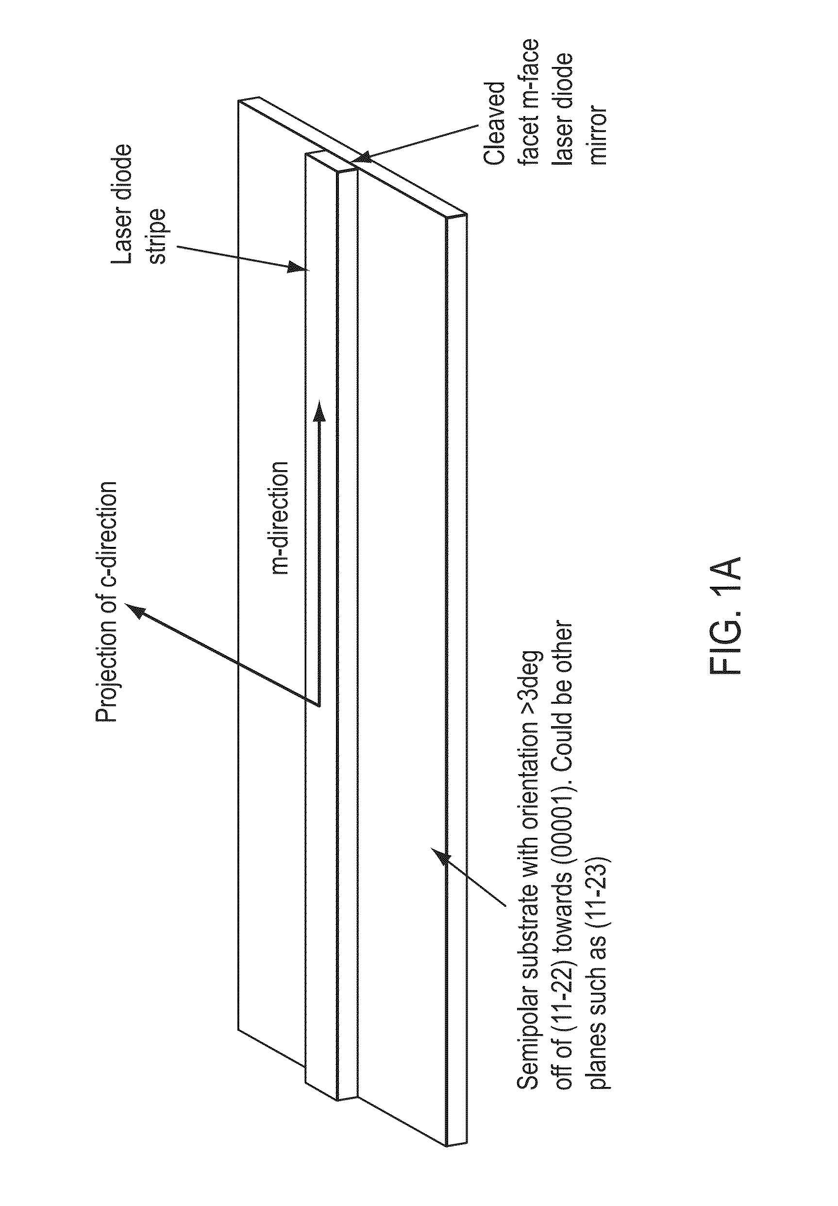
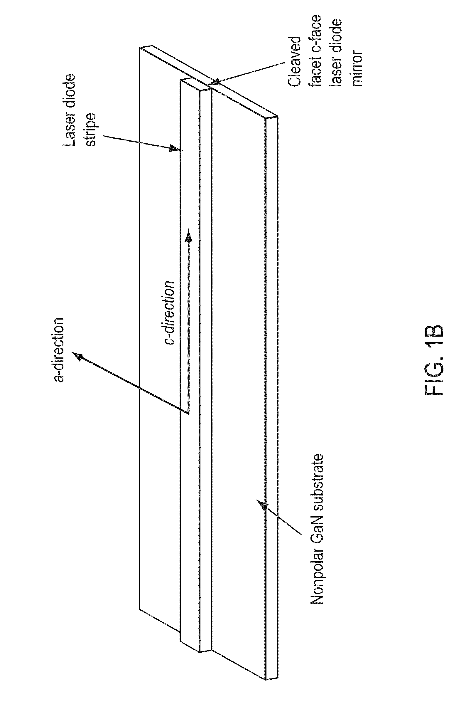
[0020]According to the present invention, techniques related generally to optical devices are provided. More particularly, the present invention provides a method and device for emitting electromagnetic radiation using semipolar or non-polar gallium containing substrates such as GaN, MN, InN, InGaN, AlGaN, and AlInGaN, and others. Merely by way of example the invention can be applied to the non-polar m-plane or to the semipolar (11-22), (30-31), (30-3-1), (20-21), (20-2-1), (30-32), or (30-3-2), or offcuts thereof. Merely by way of example, the invention can be applied to optical devices, lasers, light emitting diodes, solar cells, photoelectrochemical water splitting and hydrogen generation, photodetectors, integrated circuits, and transistors, among other devices. In a specific embodiment, the present laser device can be employed in either a semipolar or non-polar gallium containing substrate, as described below. Laser diodes according to this invention can offer improved efficien...


PUM


Abstract

Optical devices having a structured active region configured for selected wavelengths of light emissions are disclosed.

Description

CROSS-REFERENCE TO RELATED APPLICATIONS[0001]This application is a continuation-in-part of U.S. application Ser. No. 12 / 884,993 filed on Sep. 17, 2010 (Attorney Docket No. 92011-792471(001320US)), which claims priority from U.S. Provisional Application No. 61 / 249,568 filed on Oct. 7, 2009 and from U.S. Provisional Application No. 61 / 243,502 filed on Sep. 17, 2009; and this application is a continuation-in-part of U.S. application Ser. No. 12 / 778,718 filed on May 12, 2010 (Attorney Docket No. 92011-787039 (000810US)), which claims priority from U.S. Provisional Application No. 61 / 177,317 filed on May 12, 2009; and this application is a continuation-in-part of U.S. application Ser. No. 12 / 762,269 filed on Apr. 16, 2010 (Attorney Docket No. 92011-785875 (000610US)), which claims priority from U.S. Provisional Application No. 61 / 243,502 filed on Sep. 17, 2009, from U.S. Provisional Application No. 61 / 177,218 filed on May 11, 2009, from U.S. Provisional Application No. 61 / 170,550 filed o...

Claims


Application Information

Patent Timeline
IPC IPC(8): H01S5/343H01L21/18
CPCB82Y20/00H01S5/0014H01S5/0202H01S5/028H01S5/2031H01S5/3202H01S5/3213H01S5/34333H01S5/4025H01S5/2009H01S5/0287H01S5/2201H01S5/32025H01S5/320275H01S5/1085
Inventor RARING, JAMES W.
Owner KYOCERA SLD LASER INC
Why Eureka
Try Eureka