CMOS imaging device with three-dimensional architecture

a three-dimensional architecture and imaging device technology, applied in the direction of radio frequency controlled devices, instruments, transistors, etc., can solve the problems of not being able to obtain junction capacitance values, not being able to produce high-performance imaging devices comprising pixels of small size,

Inactive Publication Date: 2013-02-28
COMMISSARIAT A LENERGIE ATOMIQUE ET AUX ENERGIES ALTERNATIVES
View PDF1 Cites 14 Cited by
  • Summary
  • Abstract
  • Description
  • Claims
  • Application Information

AI Technical Summary

Problems solved by technology

Nevertheless, such a conception does not make it possible to produce a high performance imaging device comprising pixels of small size, for example of dimensions less than or equal to around 2 μm (this dimension corresponding to the dimension of a side of a square shaped pixel).
However, such a device does not make it possible to obtain such values in terms of junction capacitances.

Method used


Image

  • CMOS imaging device with three-dimensional architecture
  • CMOS imaging device with three-dimensional architecture
  • CMOS imaging device with three-dimensional architecture

Examples


first embodiment

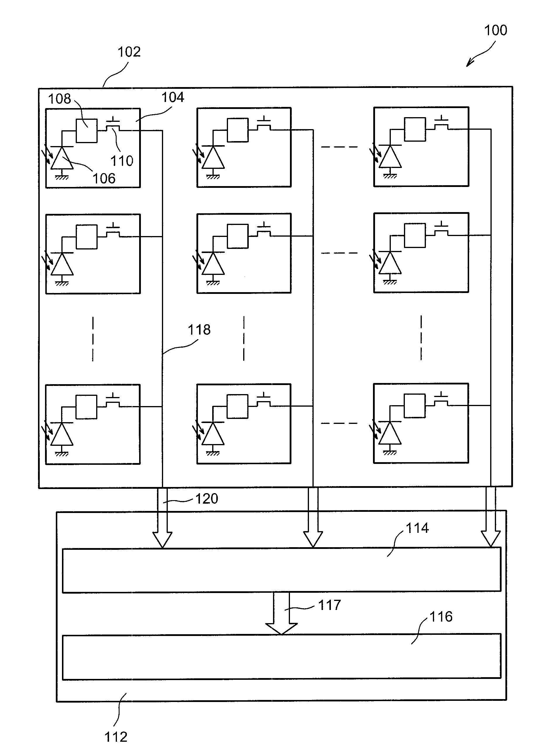
[0053]Reference is firstly made to FIG. 1 which schematically and partially represents an imaging device 100 according to a

[0054]The imaging device 100 comprises a first substrate 102, for example composed of a semi-conductor material such as silicon, on which is formed a detection circuit of the imaging device 100 formed by a plurality of pixels 104 laid out in the form of an array of n lines and m columns.

[0055]Although in FIG. 1 only nine pixels 104 are represented, the imaging device 100 comprises a much greater number of pixels 104, for example several million or several tens of million. In the example of FIG. 1, the pixels 104 each have a square shape, the sides of which have a dimension substantially equal or less than around 2 μm.

[0056]Each pixel 104 comprises a photodetector, for example a photodiode 106, intended to convert the energy of incident photons received by each of the pixels 104 into electron-hole pairs.

[0057]In a variant, the photodetectors of the imaging device...

second embodiment

[0078]In a second embodiment, the electrical interconnections 120 may be formed by a molecular bonding performed between the two substrates 102, 112, the electrical contacts of the two substrates 102 and 112 then joined together by said bonding. Such a molecular bonding is obtained by carrying out firstly a planarization of the two substrates, then placing in contact the two substrates. An annealing enables the join between the two substrates 102 and 112 to be made.

[0079]Whatever the technique used to join the first substrate 102 to the second substrate 112, or even if it is wished that the two substrates 102 and 112 are not joined to each other but simply brought close to each other, the electrical interconnections 120 may also be formed by traversing vias formed through the substrates 102 and 112.

[0080]When the electrical interconnections 120 are formed by way of beads of electrically conductive material or by carrying out a molecular bonding of the two substrates 102 and 112, the...

third embodiment

[0109]Reference is now made to FIG. 6, which schematically and partially represents an imaging device 300 according to a

[0110]Unlike the imaging device 100 described previously with reference to FIG. 1, each pixel 304 of the imaging device 300 comprises another MOS transistor 306 for selecting pixels, serving to select one of the columns of pixels 304. Thus, each pixel 304 of a macropixel of the imaging device 300 may be addressed individually by turning on the MOS transistors 110 and 306 of the pixel in question. Given that the imaging device 300 makes it possible to perform an individual addressing of the pixels 304, the buses 118 of a same macropixel are electrically connected to each other and the electrical link of a macropixel with the second substrate 112 is formed by way of a single electrical interconnection 120. In addition, the electrical interconnection 120 is directly connected to the electronic processing circuit 116, the multiplexing circuit used in the imaging device...


PUM


Abstract

An imaging device including: plural pixels each including a photodetector; plural reading circuits associated with the plural photodetectors, each reading circuit including a first MOS transistor charging/discharging a photodetector and a second MOS transistor converting charges to be output by the photodetector into voltage; an electronic processing circuit configured to process the voltages outputted by the reading circuits; a first substrate on which are formed the pixels and the reading circuits, and a second substrate, distinct from the first substrate, on which is formed the electronic processing circuit, the second substrate being linked electrically to the first substrate by an electrical interconnection forming an electrical link between the reading circuits and the electronic processing circuit.

Description

TECHNICAL FIELD[0001]The invention relates to the field of imaging devices, or image sensors, of CMOS type and produced in 3D technology (in three dimensions), in other words comprising an architecture formed of several superimposed substrates.[0002]The invention applies particularly to CMOS imaging devices produced in silicon technology, comprising pixels of small sizes, and able to perform optical detection in the visible domain.PRIOR ART[0003]A CMOS imaging device is an integrated circuit, conventionally constituted of an array of pixels and a control electronic.[0004]Each pixel comprises a photodetector intended to convert the energy of the incident photons received by the pixel into electron-hole pairs, an integration capacitance which stores the charges generated and several MOS transistors.[0005]The control electronic is responsible in particular for evacuating in a series manner, in other words pixel by pixel, the electrical information outputted by each pixel up to the outp...

Claims


Application Information

Patent Timeline
Patent Type & Authority Applications(United States)
IPC IPC(8): H01L27/146
CPCH01L27/14603H01L27/14609H01L27/14632H01L27/14634H01L27/14636H01L27/14641H01L27/14689H01L27/1469H01L27/14612H01L27/1464H01L27/14643H04N25/79
Inventor PEIZERAT, ARNAUDCAZAUX, YVONTCHAGASPANIAN, MICHAEL
Owner COMMISSARIAT A LENERGIE ATOMIQUE ET AUX ENERGIES ALTERNATIVES
Why Eureka
Try Eureka