Method for forming pattern and mask pattern, and method for manufacturing semiconductor device
- Summary
- Abstract
- Description
- Claims
- Application Information
AI Technical Summary
Benefits of technology
Problems solved by technology
Method used
Image

Examples
first embodiment
[0059]FIGS. 3A to 3F schematically show sectional views of various steps of a semiconductor device manufacturing method according to this invention.
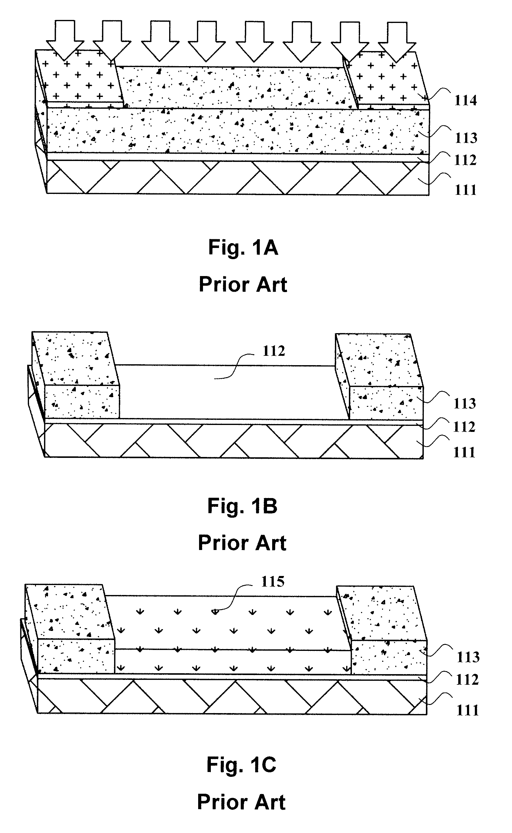
[0060]As shown in FIG. 3A, a substrate 311 is provided, a polymer thin film 313 containing a block copolymer is formed on the substrate 311, and the components of the copolymer are immiscible with each other. The block copolymer can be biblock copolymer, such as PS-b-PMMA (poly(styrene-b-methyl methacrylate)). In one embodiment, the substrate 311 comprises a mask layer 312 disposed under the polymer thin film 313. The label 320 represents a stamp, which is formed of, for example, Si, SiO2, silicon nitride, or diamond materials.
[0061]As shown in FIG. 3B, a first pattern 330 of the polymer thin film 313 is formed through imprinting the polymer thin film 313 with the stamp 320.
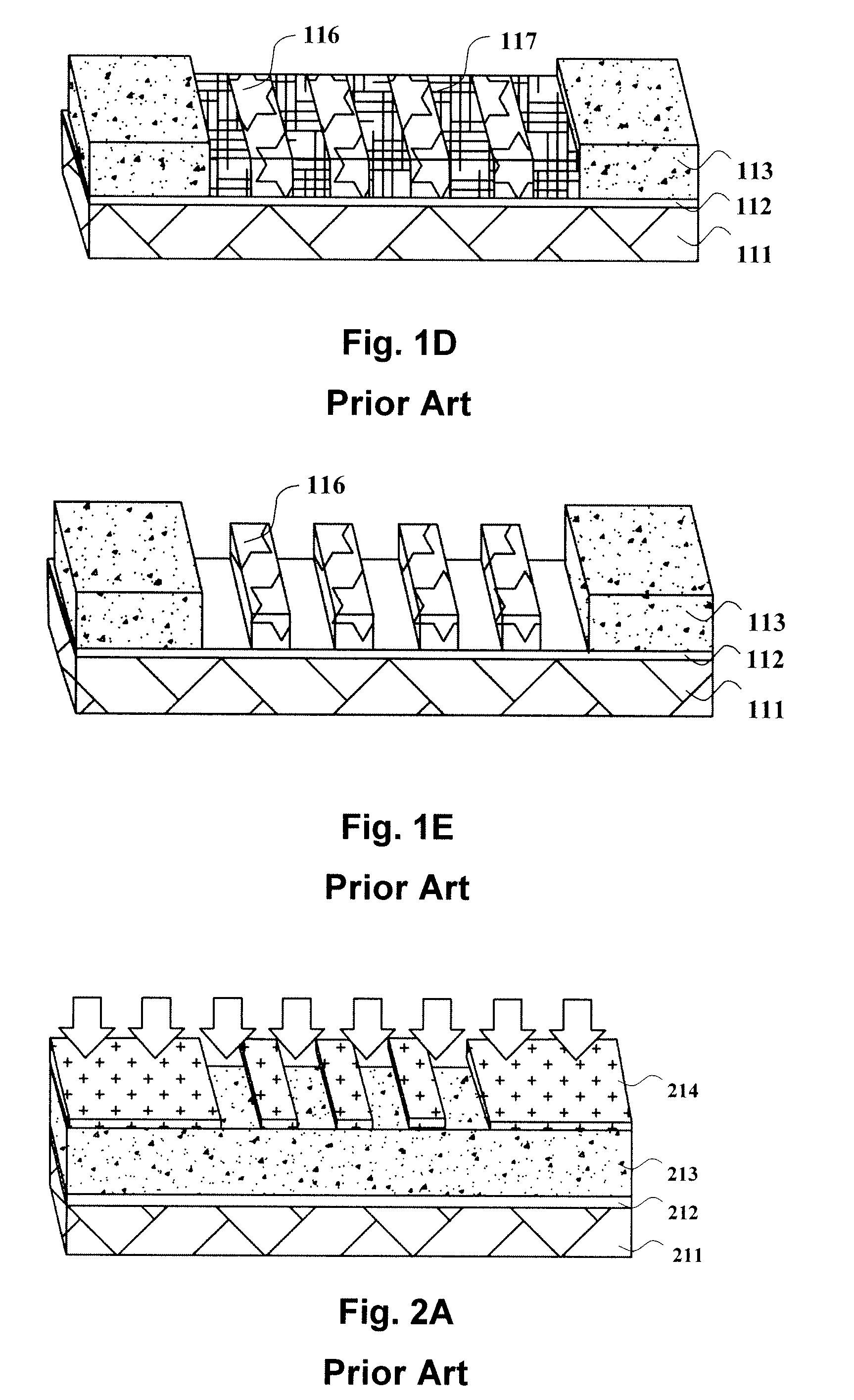
[0062]As shown in FIG. 3C, domains composed of different copolymer components, for example, domains 316 and 317 are formed respectively through directed self assembly...
second embodiment
[0070]FIGS. 4A to 4H schematically show sectional views of various steps of a semiconductor device manufacturing method according to this invention.
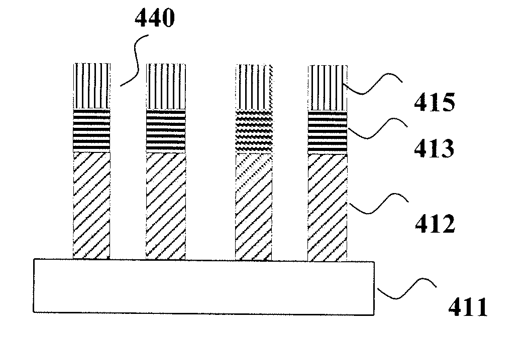
[0071]As shown in FIG. 4A, a substrate 411 is provided, with a mask layer 412 on the substrate 411, and a brush layer 413 formed on the mask layer 412. The brush layer 413, for example, is an oxygenated brush layer, and is used as a DSA template later. The brush layer can be formed through state-in-art or other methods.
[0072]As shown in FIG. 4B, a polymer thin film 414 containing a block copolymer is formed on the brush layer 413, wherein the block copolymer is, for example, PS-b-PMMA.
[0073]As shown in FIG. 4C, the polymer thin film 414 is nano-imprinted with a nano-stamp 420.
[0074]As shown in FIG. 4D, a first pattern 430 is formed on the polymer thin film 414 through imprinting.
[0075]As shown in FIG. 4E, using the brush layer 413 as a template, domains 415 and 416 composed of different copolymer components such as PS and PMMA are formed...
PUM
| Property | Measurement | Unit |
|---|---|---|
| Temperature | aaaaa | aaaaa |
| Flow rate | aaaaa | aaaaa |
| Electric field | aaaaa | aaaaa |
Abstract
Description
Claims
Application Information