Optical modulator

a technology of optical modulator and carrier density modulation, applied in optics, instruments, electrical equipment, etc., can solve the problems of low optical modulation efficiency, many of such optical modulators studied, and the device is vulnerable, so as to reduce the size of the optical modulator, reduce the optical transmission loss, and increase the overlap between a light field and a carrier density modulation region.

a technology of optical modulator and carrier density modulation, applied in optics, instruments, electrical equipment, etc., can solve the problems of low optical modulation efficiency, many of such optical modulators studied, and the device is vulnerable, so as to reduce the size of the optical modulator, reduce the optical transmission loss, and increase the overlap between a light field and a carrier density modulation region.

US20130064491A1Active Publication Date: 2013-03-14NEC CORP

Image

  • Optical modulator
  • Optical modulator
  • Optical modulator

Examples


Embodiment Construction

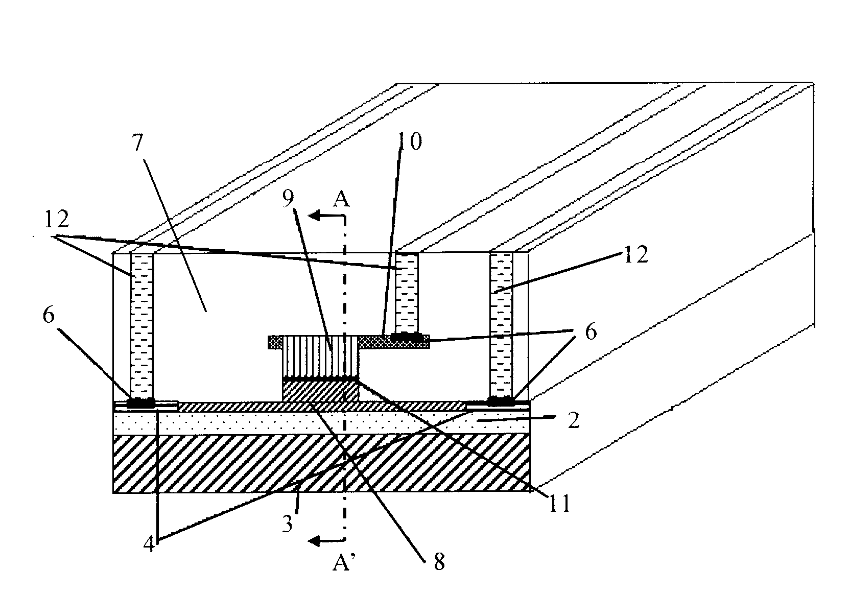
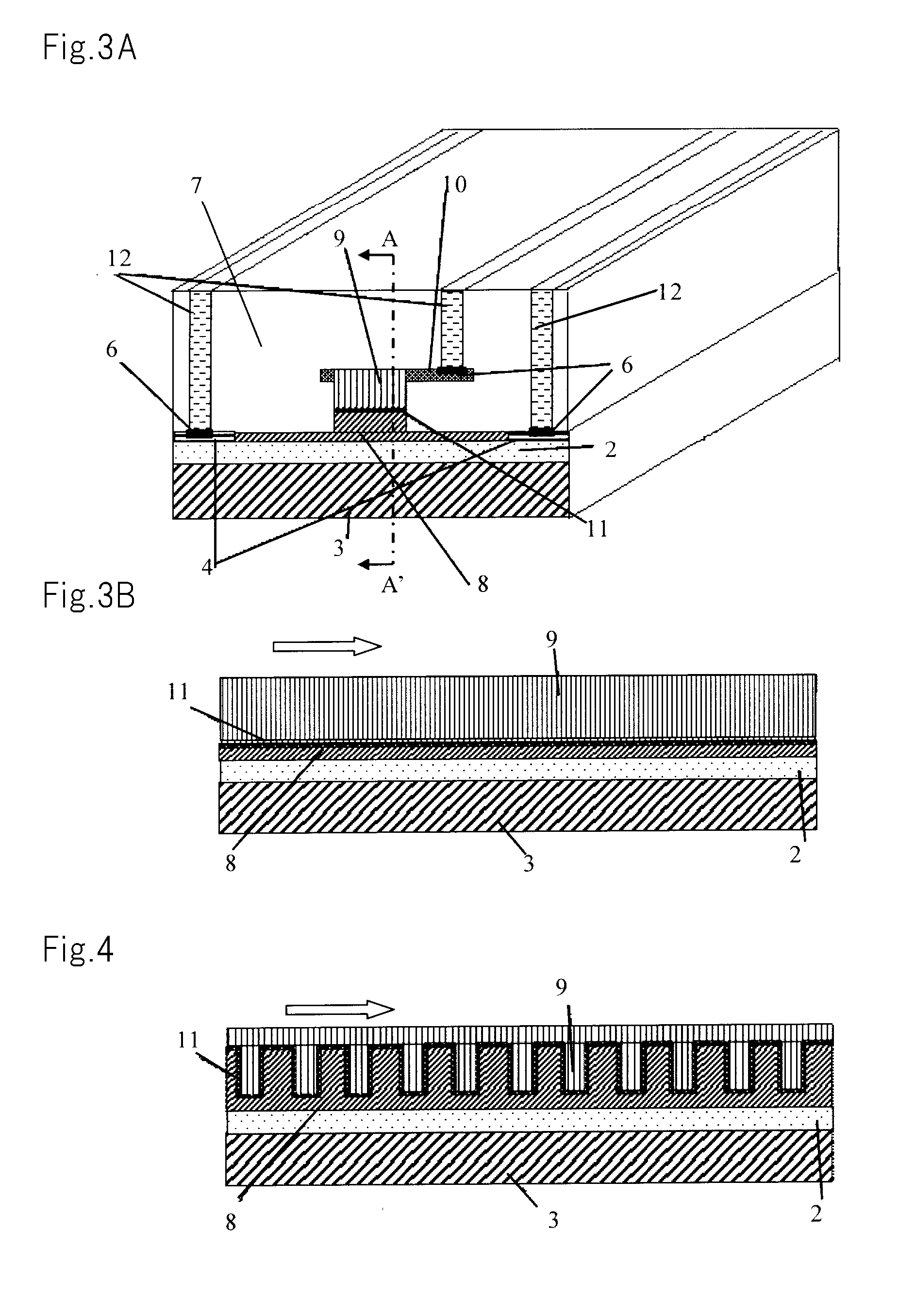
[0040]Exemplary embodiments of the present invention will be described with reference to the accompanying drawings. Components having the same functions are indicated by the same reference numerals in the drawings and the descriptions of them may be omitted.

[0041]A mechanism to modulate the carrier density in a silicon layer, which is the basis for the operation of the present invention, will be described before the description of an illustrative example of a structure for an optical modulator according to the present invention. A silicon-based optical modulator according to the present invention uses a carrier plasma effect described below.

[0042]No change due to the Pockels effect is observed in the refractive index of pure silicon, and a change in refractive index of pure silicon due to the Franz-Keldysh effect or the Kerr effect is extremely small, as described above. Therefore only a carrier plasma effect and a thermo-optic effect can be used for the optical modulation operation...


PUM

PropertyMeasurementUnit
thicknessaaaaaaaaaa
wavelengthsaaaaaaaaaa

Abstract

To provide an optical modulator having a reduced size and reduced power consumption and capable of being easily connected to a waveguide and a method of manufacturing the optical modulator. The optical modulator has at least semiconductor layer (8) having a rib-shaped portion and doped so as to be of a first conduction type, dielectric layer (11) laid on first-conduction-type semiconductor layer (8), and semiconductor layer (9) laid on dielectric layer (11), having the width at the side opposite from dielectric layer (11) increased relative to the width of the rib-shaped portion, and doped so as to be of a second conduction type.

Description

TECHNICAL FIELD [0001]The present invention relates to an optical modulator that converts into an optical signal a high-speed electrical signal required in the information processing and communication field and to a method of manufacturing the optical modulator. More particularly, the present invention relates to an optical modulator that uses a silicon-insulator-silicon capacitor structure formed on a SOI (Silicon on Insulator) substrate and to a method of manufacturing the optical modulator.BACKGROUND ART [0002]Optical fiber communication that has been mainly for business use is also becoming widespread for home use. With this movement, there is a demand for a high-performance optical communication device. As optical communication devices for various optical communication systems including optical fibers for home use and local area networks (LAN), silicon-based optical communication devices capable of functioning at optical signal wavelengths of 1330 and 1500 nm exist. The silicon...

Claims


Application Information

Patent Timeline
14 Mar 2013
Publication
US20130064491A1
IPC
G02F1/035; H01L21/02
CPC
G02F1/025; H01L21/02; G02F1/035
Inventors
FUJIKATA, JUNICHI; SAITOH, MOTOFUMI