Organic el display and method of manufacturing organic el display

a technology of organic el and display, which is applied in the direction of sustainable manufacturing/processing, final product manufacturing, thermoelectric devices, etc., can solve the problems of high luminance, high speed responsibility, and inability to obtain high luminan

Inactive Publication Date: 2013-03-21
SUMITOMO BAKELITE CO LTD
View PDF1 Cites 13 Cited by
  • Summary
  • Abstract
  • Description
  • Claims
  • Application Information

AI Technical Summary

Benefits of technology

[0021]The invention is to provide a large-size, high-accuracy organic EL display using a plastic substrate and a method of manufacturing an organic EL display using a roll-shaped long plastic substrate.

Problems solved by technology

Therefore, there is a limitation in that high luminance may not be obtained.
Therefore, if an aperture ratio of the display is considered, in the case of the organic EL display, the size of the TFT becomes an important problem in comparison with the case of a liquid crystal display.
In this case, if an a-Si TFT is used as the TFT, since the field effect mobility is about 0.5 cm2 / Vs, in the case where the area of the pixel is large or the case where the number of scan electrodes is large, for example, 2,000 or more, there is a problem in terms of high-speed responsibility and high luminance.
However, the aperture ratio of the pixel is decreased, so that high luminance may not be implemented.
Therefore, a sufficient time for charging the holding capacitance may not be secured, so that turning on of the TFT may not be satisfactorily performed.
In addition, in the a-Si TFT, a change in the reverse voltage Vt due to current stress is large, so that the occurrence of unbalance of the driving current is inevitable for a long time of the driving.
In the organic EL device, the unbalance of the driving current leads to irregularity in luminance.
In addition, with respect to the low-temperature p-Si TFT, since the manufacturing process temperature is high, from 500° C. to 600° C., the plastic substrate may not be used.
Therefore, it is difficult to implement a flexible display.

Method used


Image

  • Organic el display and method of manufacturing organic el display
  • Organic el display and method of manufacturing organic el display
  • Organic el display and method of manufacturing organic el display

Examples


first embodiment

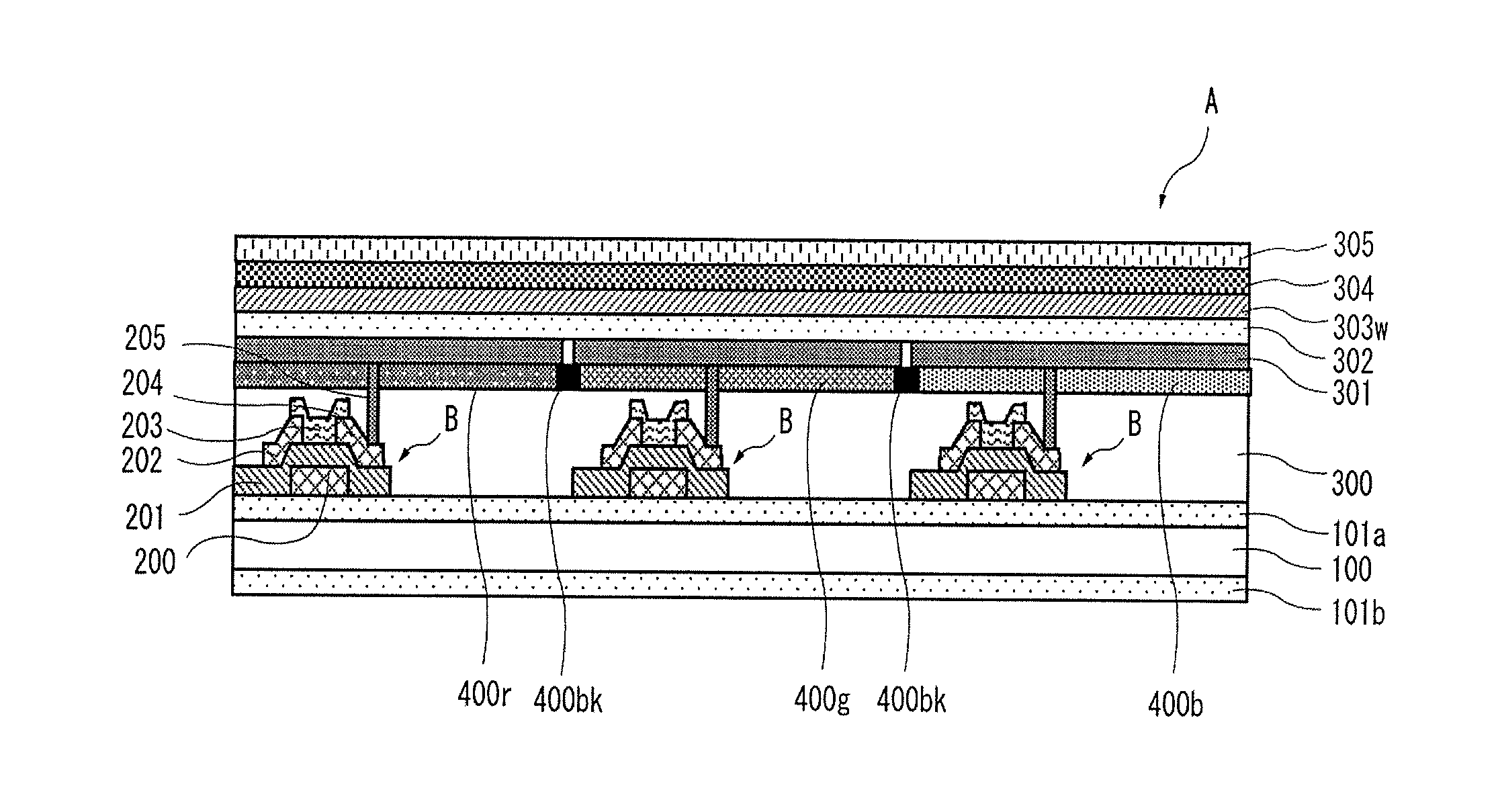
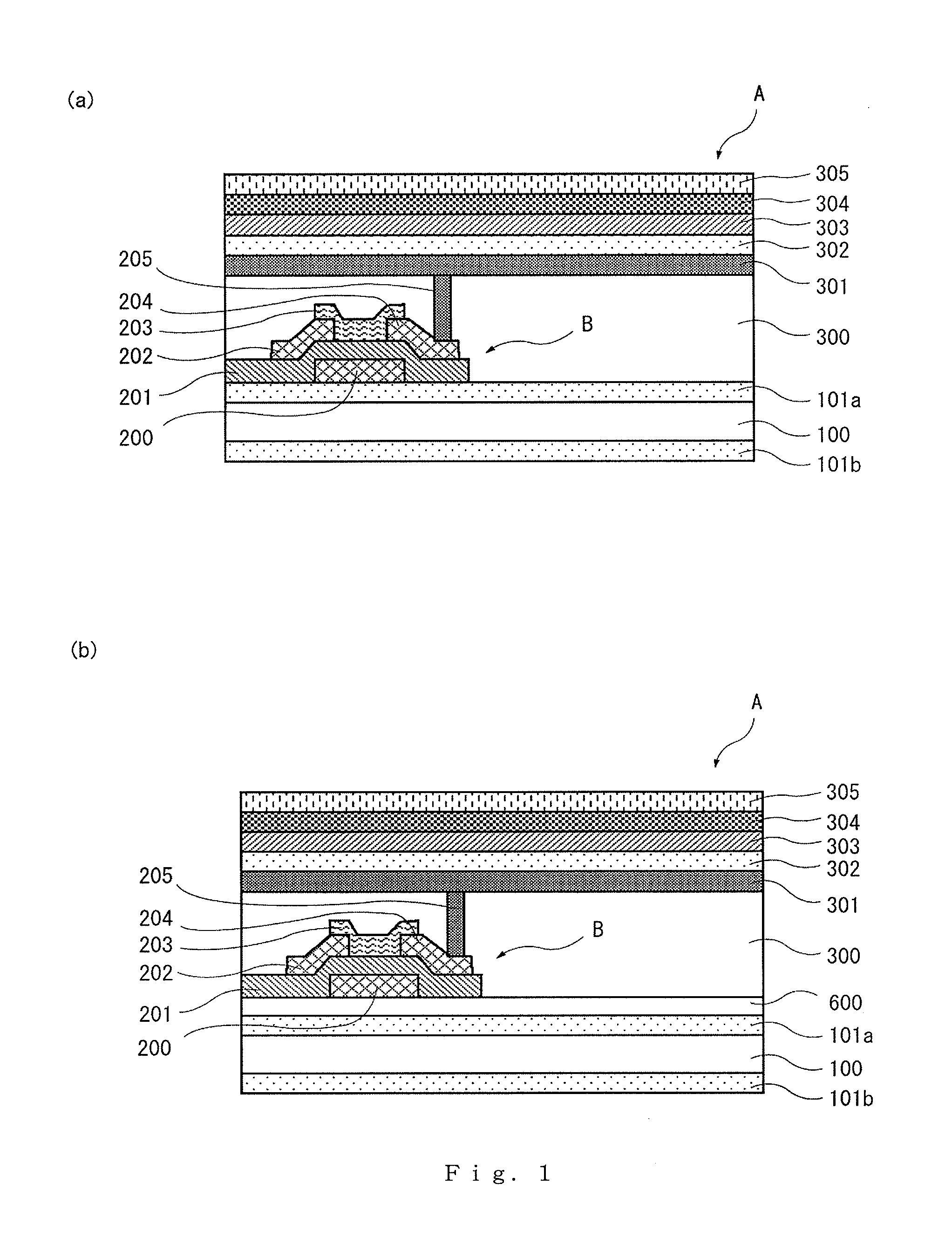
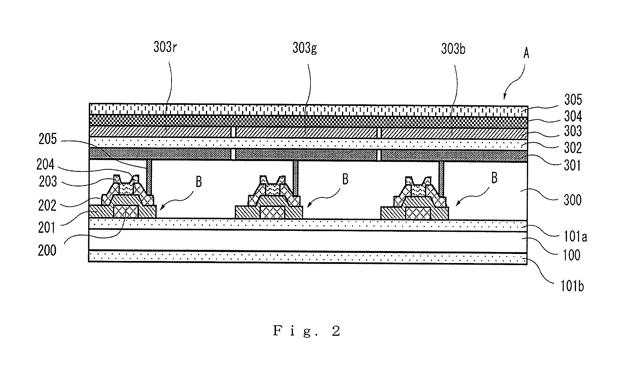
[0093]FIG. 5 is a process flowchart illustrating a method of manufacturing an organic EL display. The method according to the embodiment includes a gas barrier layer forming process S1, a thin film transistor forming process S2, and organic EL device portion forming process S3. In the gas barrier layer forming process S1, gas barrier layers 101a and 101b are formed on a transparent plastic substrate 100 which has a shape of a long roll.

[0094]In the thin film transistor forming process S2, an active layer 203 containing a non-metallic element which is a mixture of oxygen (O) and nitrogen (N) and has a ratio of N to O (N number density / O number density) from 0 to 2 is formed on the gas barrier layer 101a through a sputtering method.

[0095]In the organic EL device portion forming process S3, a lower electrode 301 which is a positive electrode of the organic EL device A, a hole transport layer 302, a light emitting layer 303, an electron transport layer 304, and an upper electrode 305 wh...

second embodiment

[0126]Although the configuration of the second embodiment is similar to that of the first embodiment, the organic EL device portion forming process S3 includes a process of forming layers of emitting light of at least three primary colors of red (R), green (G), and blue (B) in the organic EL device A. In the case where full-color display is performed by an organic EL display C, a configuration for emitting light of at least three primary colors of red (R), green (G), and blue (B) is needed. In this case, since the emitted light of the organic EL device A is directly used as it is, the light use efficiency is the highest among full-color display methods, which is preferable. A configuration for emitting light of four colors or six colors including white (W), yellow (Y), cyan (C), and the like in addition to RGB may be used.

third embodiment

[0127]Although the configuration of the third embodiment is similar to that of the first embodiment, the organic EL device portion forming process S3 includes a process of forming at least a white light emitting layer and a color filter layer in the organic EL device A. Instead of emitting light of three primary colors or light of four colors to six colors, full color display can be made by using a white light emitting layer and a color filter layer. In this case, since only a single white light emitting layer may be formed as the light emitting layer, there is no need to form separate light emitting layers for different colors of the emitted light. Therefore, the number of processes can be reduced, and the manufacturing apparatus is more simplified, so that it is effective in that the manufacturing can be performed with a more inexpensive apparatus. Similarly to a color liquid crystal panel, the full color display is performed by allowing the light from the white light emitting lay...


PUM


Abstract

It is possible to manufacture a large-size, high-accuracy organic EL display using a plastic substrate and an organic EL display using a roll-shaped long plastic substrate.The organic EL display includes an organic EL device A having at least a lower electrode 300, an organic layer including at least a light emitting layer, and an upper electrode 305 and a thin film transistor B on a transparent plastic substrate 100, a source electrode or drain electrode of the thin film transistor B is connected to the lower electrode 300, the plastic substrate 100 has a gas barrier layer 101a, the thin film transistor B is formed on the gas barrier layer 101a, the thin film transistor B includes an active layer 203 containing a non-metallic element which a mixture of oxygen (O) and nitrogen (N) and has a ratio of N to O (N number density / O number density) from 0 to 2, and the organic EL device A is formed at least on the gas barrier layer 101a or one the thin film transistor B.

Description

BACKGROUND OF THE INVENTION[0001]1. Field of the Invention[0002]The present invention relates to an organic EL display which is formed by using, particularly, a plastic substrate and is driven by a thin film transistor including an active layer containing a non-metallic element and a method of manufacturing the organic EL display.[0003]2. Description of the Related Art[0004]Recently, as development of technologies for materials, manufacturing, driving circuits, and the like, a technology for electroluminescence (EL) has been put to practical use of an organic EL display as one of flat panel displays (FPDs).[0005]In 1997, a monochromatic organic EL display was put to practical use. After that, area colorization of the organic EL display is implemented, so that the use thereof is expended to displays such as a small-size audio apparatus or a mobile terminal. In 2001, the colorization was put to practical use by a passive-matrix-type color display for a mobile phone. After that, an act...

Claims


Application Information

Patent Timeline
Patent Type & Authority Applications(United States)
IPC IPC(8): H01L51/52H01L33/08
CPCH01L27/1225H01L27/3211H01L27/3262H01L29/78603H01L29/7869H01L51/0097H01L27/322H01L2251/5338H01L2251/55Y02E10/549H01L29/66969H01L27/1218H01L51/5253Y02P70/50H10K59/35H10K59/38H10K59/1213H10K77/111H10K2101/00H10K50/844H10K2102/311H01L29/06H01L29/66742
Inventor OTSUKI, SHIGEYOSHIEGUCHI, TOSHIMASAYAMAGUCHI, SHINYAOKAMOTO, MAMORU
Owner SUMITOMO BAKELITE CO LTD
Why Eureka
Try Eureka