Check patentability & draft patents in minutes with Patsnap Eureka AI!

Acoustic sensor, acoustic transducer, microphone using the acoustic transducer, and method for manufacturing the acoustic transducer

Active Publication Date: 2013-03-21
ORMON CORPORATION +1
View PDF7 Cites 13 Cited by
  • Summary
  • Abstract
  • Description
  • Claims
  • Application Information

AI Technical Summary

Benefits of technology

The present invention is related to an acoustic transducer with a surface that has an impurity added to it. The impurity can be any substance that can modify the surface of the semiconductor substrate, such as a dopant or a chemical. By adding the impurity, the surface of the semiconductor can be made more resistant to light damage. This reduces the number of electrons and holes generated by the light, which in turn reduces the electric current and the noise it generates. As a result, the acoustic transducer can detect pressure more accurately.

Problems solved by technology

This leads to change in capacitance of the capacitor formed by the vibrating membrane and the fixed electrode.

Method used


Image

  • Acoustic sensor, acoustic transducer, microphone using the acoustic transducer, and method for manufacturing the acoustic transducer
  • Acoustic sensor, acoustic transducer, microphone using the acoustic transducer, and method for manufacturing the acoustic transducer
  • Acoustic sensor, acoustic transducer, microphone using the acoustic transducer, and method for manufacturing the acoustic transducer

Examples


Embodiment Construction

[0036]An embodiment of the present invention is described below with reference to FIGS. 1 through 11.

[0037](Structure of an Acoustic Sensor)

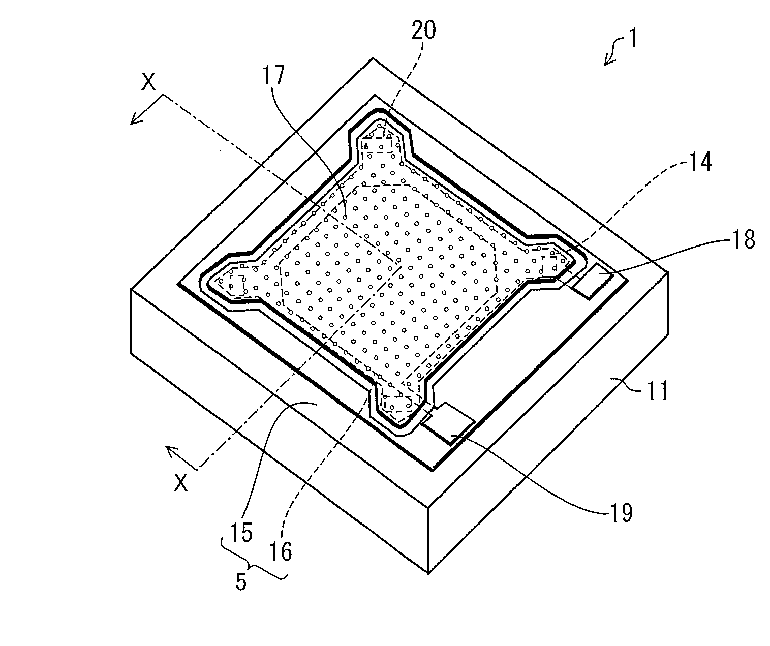
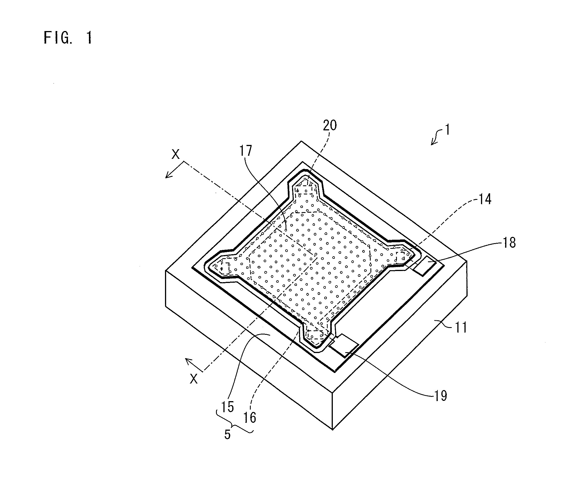
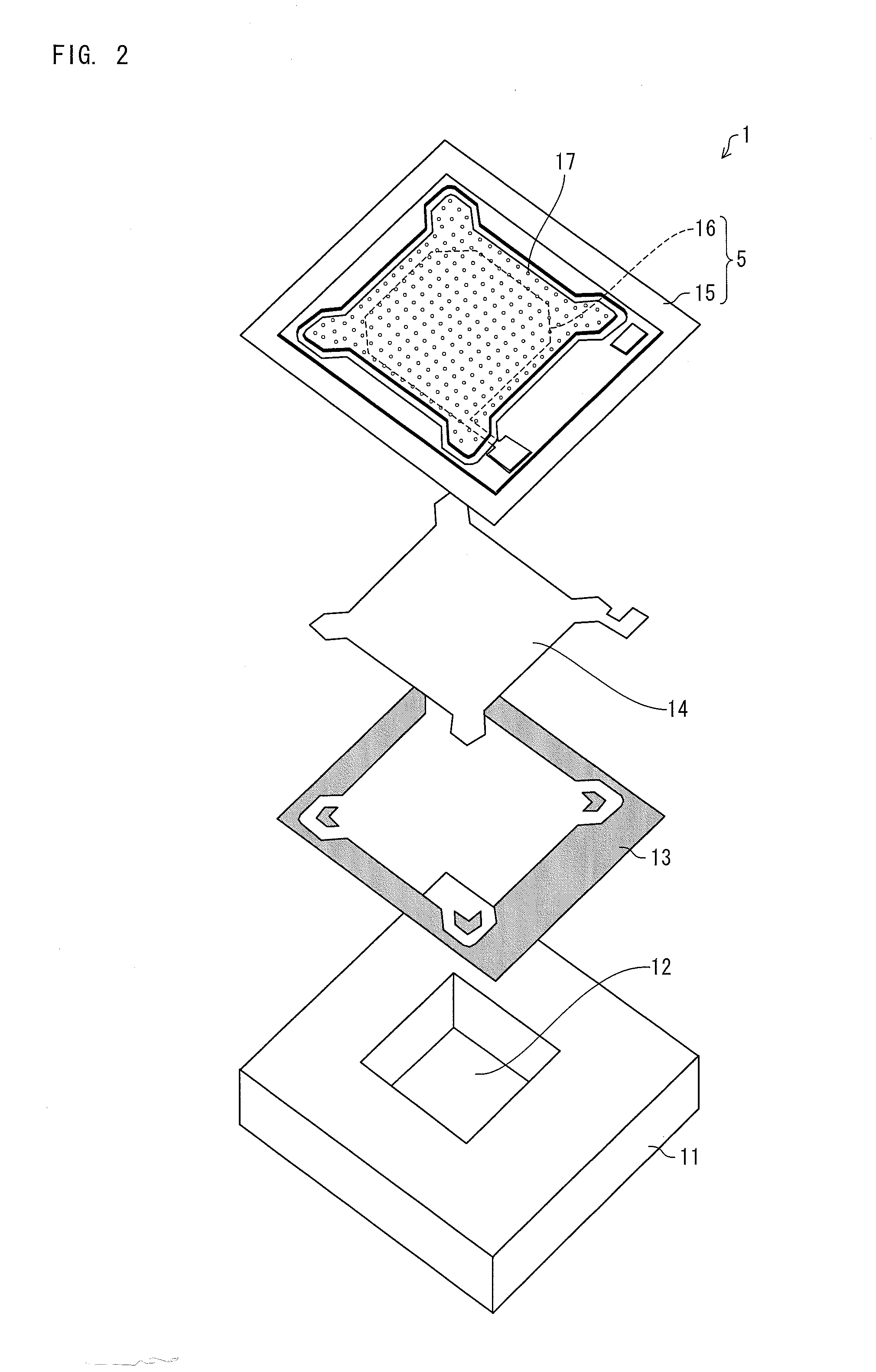
[0038]First, a structure of an acoustic sensor (acoustic transducer) 1 according to the present embodiment is described with reference to FIGS. 1 through 3. FIG. 1 is a perspective view showing an external appearance of the acoustic sensor 1. Further, FIG. 2 is an exploded perspective view of the acoustic sensor 1. Furthermore, FIG. 3 includes a cross-sectional view of the acoustic sensor 1. (a) of FIG. 3 is an cross-sectional view of the acoustic sensor 1 as taken along the line X-X of FIG. 1. (b) of FIG. 3 is an enlarged view of a region 31 of (a) of FIG. 3, and (c) of FIG. 3 is an enlarged view of a region 32 of (a) of FIG. 3.

[0039]As shown in FIGS. 1 and 2, the acoustic sensor 1 includes: a silicon substrate (semiconductor substrate) 11 provided with a through hole serving as a back chamber 12; an insulating membrane 13 stacked on the silico...


PUM


Abstract

In an acoustic sensor, a conductive vibrating membrane and a fixed electrode plate are disposed above a silicon substrate with an air gap provided therebetween, and the substrate has an impurity added to a surface thereof. A microphone includes an acoustic transducer; and an acquiring section that acquires a change in pressure as detected by the acoustic transducer. A method for manufacturing an acoustic transducer including a semiconductor substrate, a vibrating membrane, which is conductive, and a fixed electrode plate and detecting a pressure according to a change in capacitance between the vibrating membrane and the fixed electrode plate, the method includes an impurity adding step of adding an impurity to a surface of the semiconductor substrate; and a forming step of forming the vibrating membrane and the fixed electrode plate above the semiconductor substrate to which the impurity has been added.

Description

TECHNICAL FIELD[0001]The present invention relates to acoustic transducers and, in particular, to an acoustic transducer with a micro size, which is manufactured by using a MEMS (Micro Electro Mechanical System) technique, to a microphone using the acoustic transducer, and to a method for manufacturing the acoustic transducer.BACKGROUND ART[0002]Conventionally, a microphone using an acoustic sensor, called an ECM (Electret Condenser Microphone), has been used as a small-sized microphone. However, the ECM is weak against heat, and a microphone (MEMS microphone) using an acoustic sensor manufactured by using a MEMS technique is superior in terms of coping with digitalization, of miniaturization, of enhancement of functionality / multi-functionality, and of power saving. Accordingly, in recent years, the MEMS microphone is being often employed.[0003]The acoustic sensor (MEMS sensor) manufactured by using the MEMS technique is an acoustic sensor fabricated by using a semiconductor integra...

Claims


Application Information

Patent Timeline
IPC IPC(8): H01L29/84H01L21/02
CPCH04R19/005H04R2410/03H04R19/04H04R31/00
Inventor ISHIMOTO, KOICHITATARA, YOSHITAKAINUZUKA, SHINCONTI, SEBASTIANO
Owner ORMON CORPORATION
Features
  • R&D
  • Intellectual Property
  • Life Sciences
  • Materials
  • Tech Scout
  • Unparalleled Data Quality
  • Higher Quality Content
  • 60% Fewer Hallucinations
Learn More