Power semiconductor devices and fabrication methods

a technology of power semiconductors and fabrication methods, applied in semiconductor devices, instruments, electrical appliances, etc., can solve the problems of increased on-state losses, increased voltage drop in on-state, and smaller or larger pitch between the two depletion layers, so as to reduce device on-resistance, uniform on-state behaviour, and shorten the channel

Inactive Publication Date: 2013-03-21
POWER INTEGRATIONS INC
View PDF1 Cites 40 Cited by
  • Summary
  • Abstract
  • Description
  • Claims
  • Application Information

AI Technical Summary

Benefits of technology

[0031]In preferred implementations of the method, forming both the channel region of the p-top layer and the RESURF region of the p-top layer adjacent to the n-drift region use the same mask, and preferably both the channel region and the RESURF region of the device are formed in the same processing step. This approach locks the spatial positions of the channel and RESURF regions of the device, both in the same p-top layer, with respect to one another. This helps to achieve uniform on-state behaviour from one device / wafer / lot to the next, as well as enabling the use of a shorter channel, which in turn can reduce device on-resistance.

Problems solved by technology

The parasitic JFET effect introduces an additional voltage drop in the on-state and hence higher on-state losses.
This misalignment results, however, in a smaller or larger pitch between the two depletion layers and, as a result, a smaller or larger parasitic voltage drop.
The parasitic JFET effect leads therefore to non-uniform on-state behaviour from wafer to wafer and / or lot to lot.

Method used


Image

  • Power semiconductor devices and fabrication methods
  • Power semiconductor devices and fabrication methods
  • Power semiconductor devices and fabrication methods

Examples


Embodiment Construction

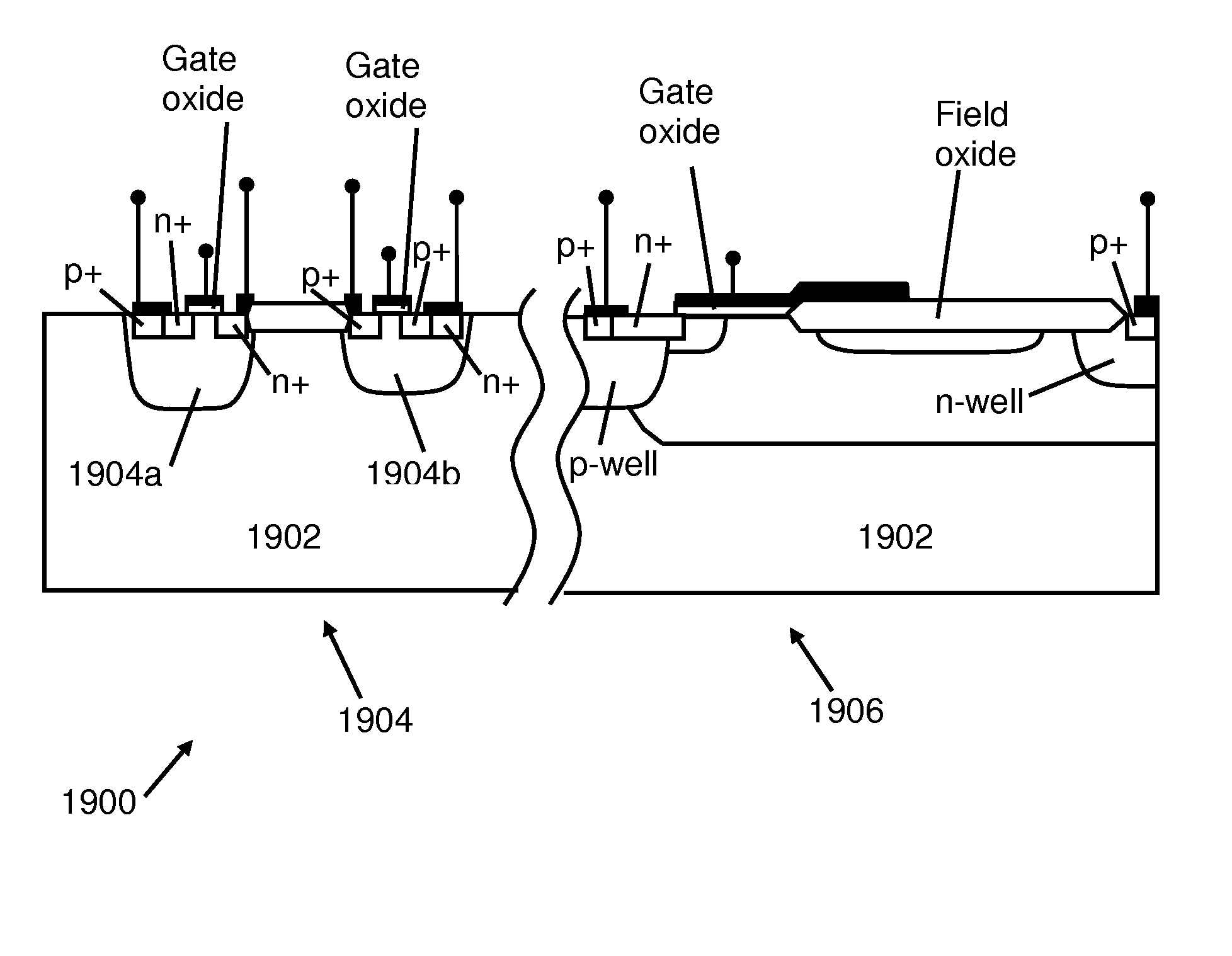
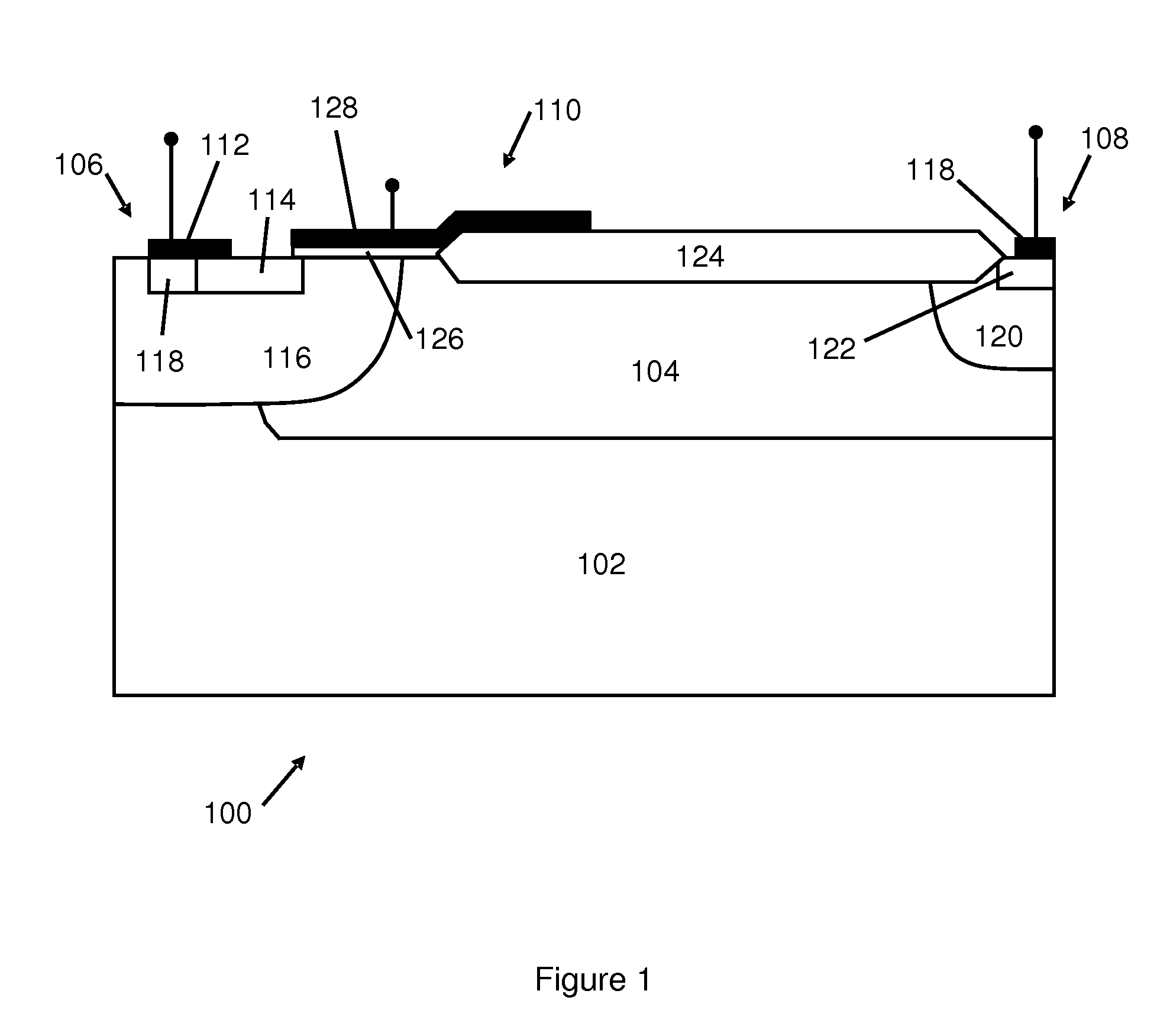
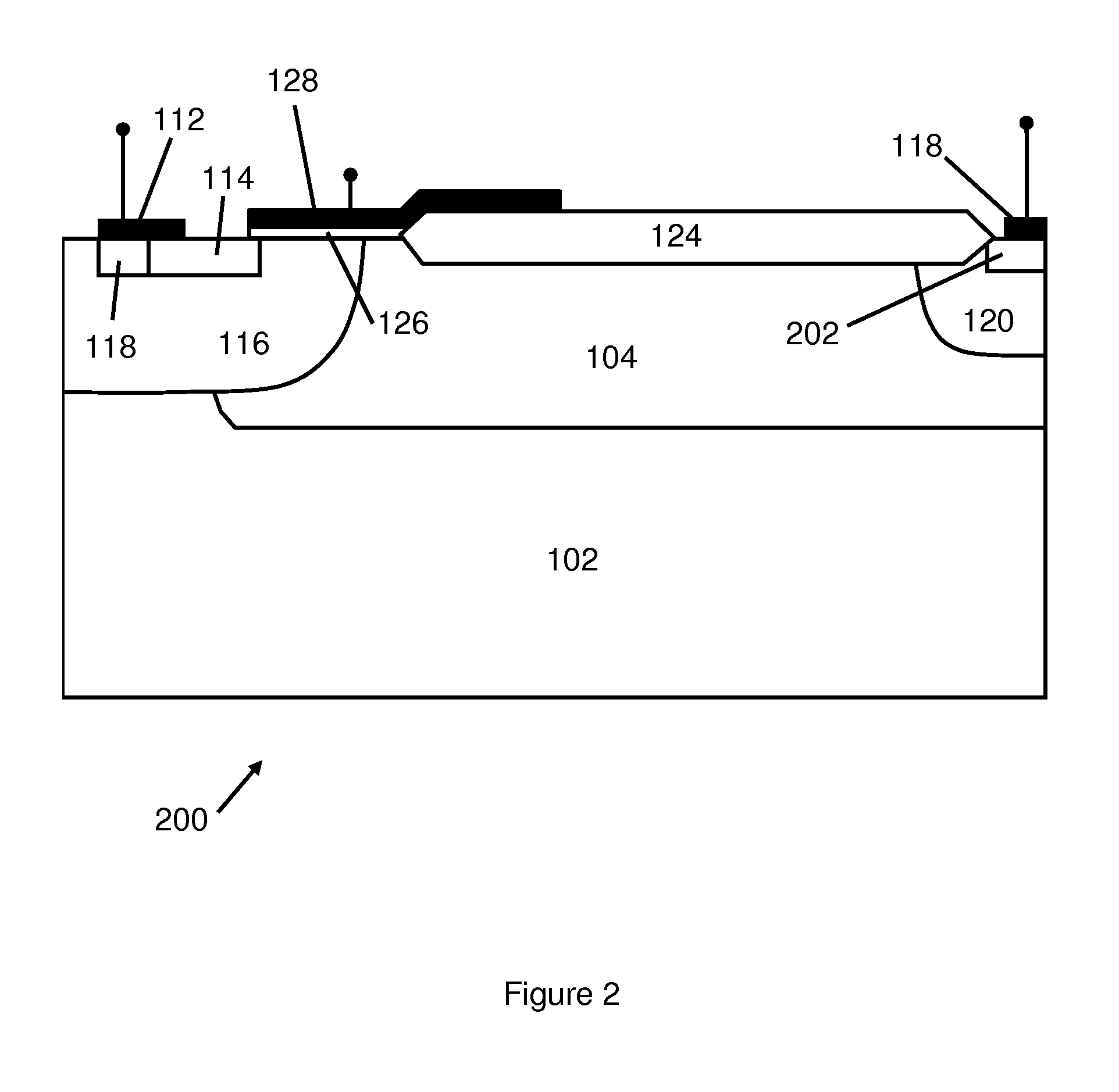
[0058]Broadly speaking we will describe a lateral high voltage device where the p-top is used both as a double RESURF layer and as the background doping for the MOS channel in a high voltage lateral device. The process of forming the p-top in the channel region does not require any additional mask layer or processing steps as it is done at the same time and using the same mask as that for the double RESURF layer.

[0059]Instead of using the p-well as the background region for the MOS channel which could result in a long lateral diffusion and therefore high channel length, the use of the p-top in the channel region leads to a shorter channel length and therefore higher transconductance for the MOS channel. The reason that the channel formed in the p-top is shorter is because the p-top is a shallower layer and hence its lateral diffusion is significantly smaller than that of the p-well. In addition, due to the fact that the p-top is a much shallower layer than the p-well, the parasitic ...


PUM


Abstract

We describe a RESURF semiconductor device having an n-drift region with a p-top layer and in which a MOS (Metal Oxide Semiconductor) channel of the device is formed within the p-top layer.

Description

FIELD OF THE INVENTION[0001]This invention relates to lateral power semiconductor devices, and more particularly to improved RESURF (REduced SURface Field) semiconductor devices and their fabrication methods. The techniques we describe are useful for high voltage semiconductor devices incorporated into power hybrid and integrated circuits. They are particularly advantageous for RESURF MOS (metal oxide semiconductor) devices such as LDMOSFETs and for MOS-bipolar transistors such as lateral insulated gate bipolar transistors (LIGBTs) incorporating RESURF.BACKGROUND TO THE INVENTION[0002]Lateral power devices typically operate with a voltage in the range 20 V to 1.2 KV. Power devices typically operate with a current in the range 10 mA to 50 A and typically higher than 0.1 A and smaller than 5 A. Such devices may also be referred to as “high voltage / power devices”. These devices are typically capable of delivering from a few milliwatts to 1 Watt or even a few tens of Watts of power. The...

Claims


Application Information

Patent Timeline
Patent Type & Authority Applications(United States)
IPC IPC(8): H01L29/78G05F3/02H01L21/336
CPCH01L29/7816H01L29/1095H01L29/42368H01L29/66325H01L29/66681H01L29/7393H01L2924/0002H01L29/7824H01L29/7835H01L29/0634H01L29/1033H01L29/1045H01L2924/00
Inventor TRAJKOVIC, TANYAUDREA, FLORINPATHIRANA, VASANTHAUDUGAMPOLA, NISHAD
Owner POWER INTEGRATIONS INC
Why Eureka
Try Eureka