Method and System for Optimization of an Image on a Substrate to be Manufactured Using Optical Lithography

a technology of optical lithography and image, applied in the field of lithography, can solve the problems of difficult to accurately translate the physical design to the actual circuit pattern developed on the resist layer, requires costly computation time, and difficult to add opc features, etc., and achieve the effect of improving the calculated substrate imag

Inactive Publication Date: 2013-03-21
D2S
View PDF2 Cites 56 Cited by
  • Summary
  • Abstract
  • Description
  • Claims
  • Application Information

AI Technical Summary

Benefits of technology

[0012]A method and system for optimization of an image to be printed on a substrate using optical lithography is disclosed in which a set of charged particle beam shots, some of which overlap, is determined so as to form a target pattern on a surface such as a reticle. Th...

Problems solved by technology

An example of an end-use limitation is defining the geometry of a transistor in a way in which it cannot sufficiently operate at the required supply voltage.
The design rule limitations reflect, among other things, the smallest dimensions that can be reliably fabricated.
As the critical dimensions of the circuit pattern become smaller and approach the resolution value of the exposure tool, the accurate transcription of the physical design to the actual circuit pattern developed on the resist layer becomes difficult.
Adding OPC features is a very laborious task, requires costly computation time, and results in more expensive reticles.
Not only are OPC patterns compl...

Method used


Image

  • Method and System for Optimization of an Image on a Substrate to be Manufactured Using Optical Lithography
  • Method and System for Optimization of an Image on a Substrate to be Manufactured Using Optical Lithography
  • Method and System for Optimization of an Image on a Substrate to be Manufactured Using Optical Lithography

Examples


Embodiment Construction

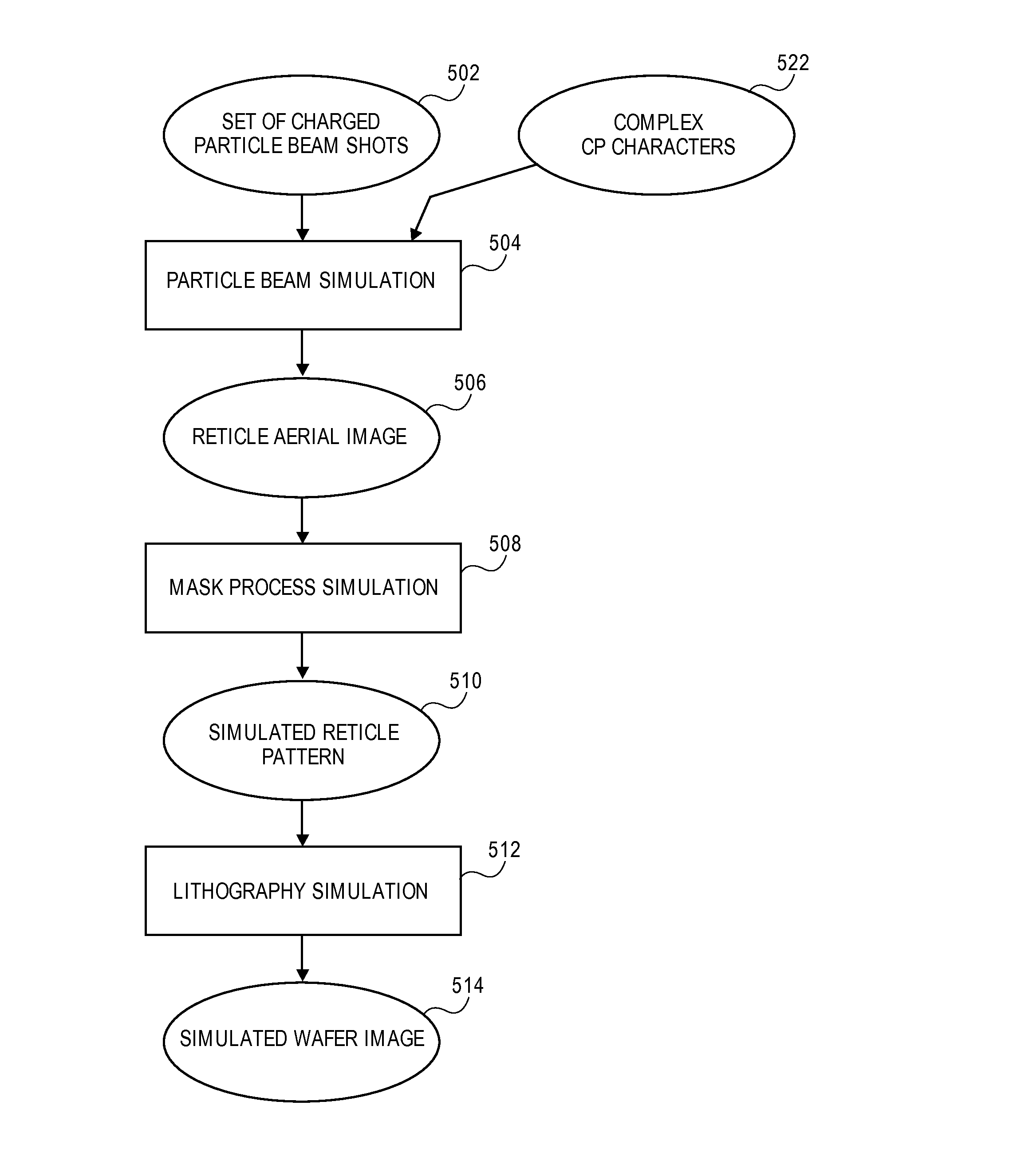
[0028]The improvements and advantages of the present disclosure can be accomplished using double simulation to determine an image that will be formed on a substrate such as a silicon wafer using an optical lithographic process, and then modifying the set of shots so as to improve or optimize the simulated substrate image.

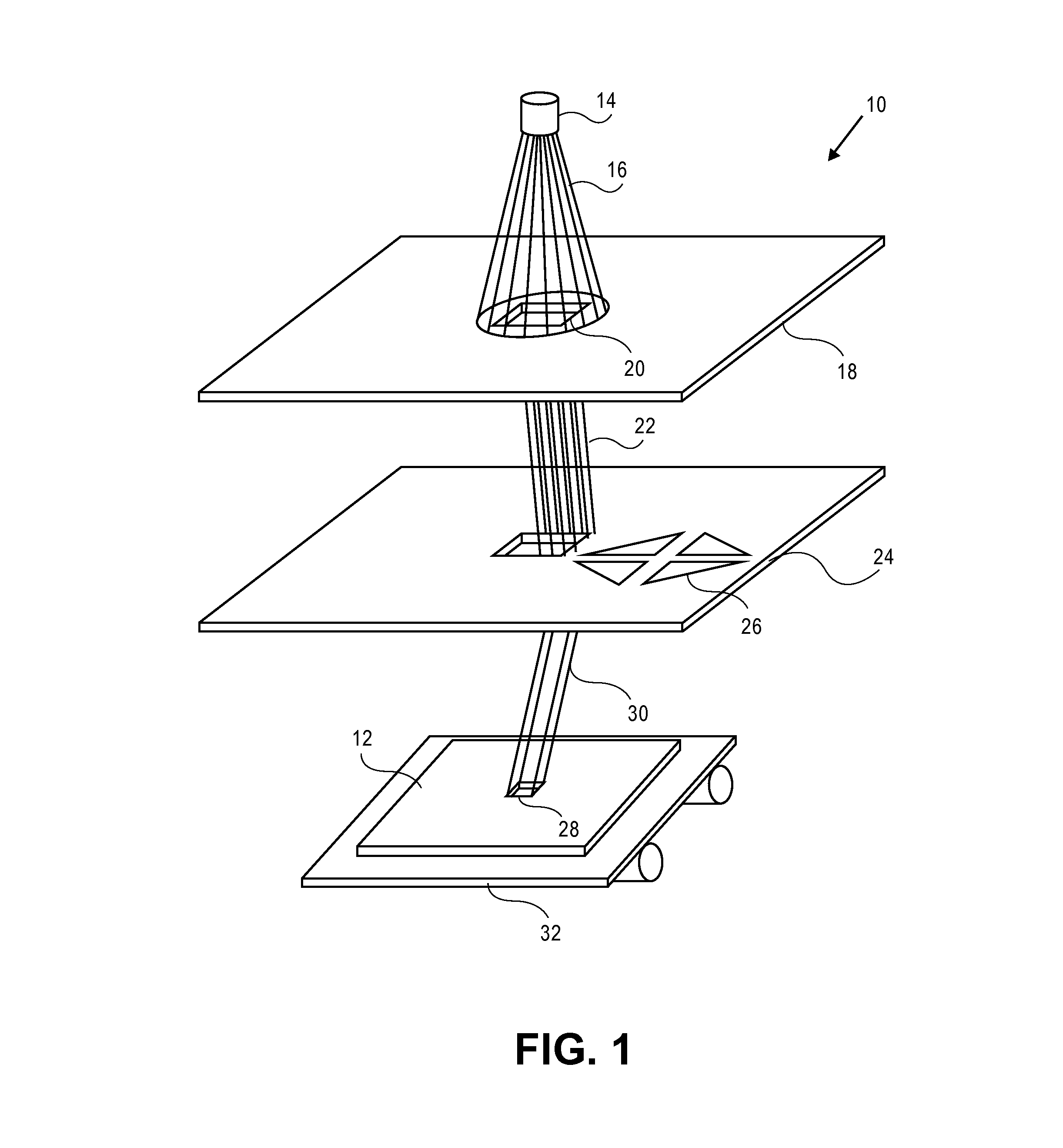
[0029]Referring now to the drawings, wherein like numbers refer to like items, FIG. 1 identifies an embodiment of a lithography system, such as a charged particle beam writer system, in this case an electron beam writer system 10, that employs a variable shaped beam (VSB) to manufacture a surface 12 according to the present disclosure. The electron beam writer system 10 has an electron beam source 14 that projects an electron beam 16 toward an aperture plate 18. The plate 18 has an aperture 20 formed therein which allows the electron beam 16 to pass. Once the electron beam 16 passes through the aperture 20 it is directed or deflected by a system of lenses (not shown...


PUM


Abstract

A method and system for optimization of an image to be printed on a substrate using optical lithography is disclosed in which a set of charged particle beam shots, some of which overlap, is determined so as to form a target pattern on a surface such as a reticle. The charged particle beam shots are simulated to determine the pattern that would be formed on the surface. Next, a substrate image is calculated from the simulated surface pattern. One or more shots in the set of shots are then modified to improve the calculated substrate image.

Description

BACKGROUND OF THE DISCLOSURE[0001]The present disclosure is related to lithography, and more particularly to the design and manufacture of a surface which may be a reticle, a wafer, or any other surface, using charged particle beam lithography.[0002]In the production or manufacturing of semiconductor devices, such as integrated circuits, optical lithography may be used to fabricate the semiconductor devices. Optical lithography is a printing process in which a lithographic mask or photomask manufactured from a reticle is used to transfer patterns to a substrate such as a semiconductor or silicon wafer to create the integrated circuit (I.C.). Other substrates could include flat panel displays, holographic masks, or even other reticles. While conventional optical lithography uses a light source having a wavelength of 193 nm, extreme ultraviolet (EUV) or X-ray lithography are also considered types of optical lithography in this application. The reticle or multiple reticles may contain ...

Claims


Application Information

Patent Timeline
IPC IPC(8): G03B27/42
CPCG03F1/36G03F7/70441H01J2237/31776H01J2237/31764H01J2237/31771G03F7/705H01L21/0274
Inventor FUJIMURA, AKIRA
Owner D2S
Why Eureka
Try Eureka