Thin-film semiconductor device for display apparatus, method for manufacturing thin-film semiconductor device for display apparatus, el display panel, and el display apparatus

Active Publication Date: 2013-04-04
JOLED INC
View PDF12 Cites 13 Cited by
  • Summary
  • Abstract
  • Description
  • Claims
  • Application Information

AI Technical Summary

Benefits of technology

The present disclosure describes a thin-film semiconductor device for display apparatus that solves problems associated with traditional devices. By having separate layers for the gate line and gate electrode, different materials can be used for each, reducing costs. Additionally, the base layer containing the power supply line and the thin-film transistors are in the same layer, which improves flatness. The layout of the thin-film transistors is more flexible, and the semiconductor layer can be larger, which increases the transistor width even if the mobility of carriers is low. These technical effects improve the performance and flexibility of the thin-film semiconductor device for display apparatus.

Problems solved by technology

In the gate line 921, high line resistivity causes delay in signals or uneven display due to voltage drop.
Particularly, increased driving frequency due to increased panel dimension makes the panel more likely to be affected by the line resistance.

Method used


Image

  • Thin-film semiconductor device for display apparatus, method for manufacturing thin-film semiconductor device for display apparatus, el display panel, and el display apparatus
  • Thin-film semiconductor device for display apparatus, method for manufacturing thin-film semiconductor device for display apparatus, el display panel, and el display apparatus
  • Thin-film semiconductor device for display apparatus, method for manufacturing thin-film semiconductor device for display apparatus, el display panel, and el display apparatus

Examples


first embodiment

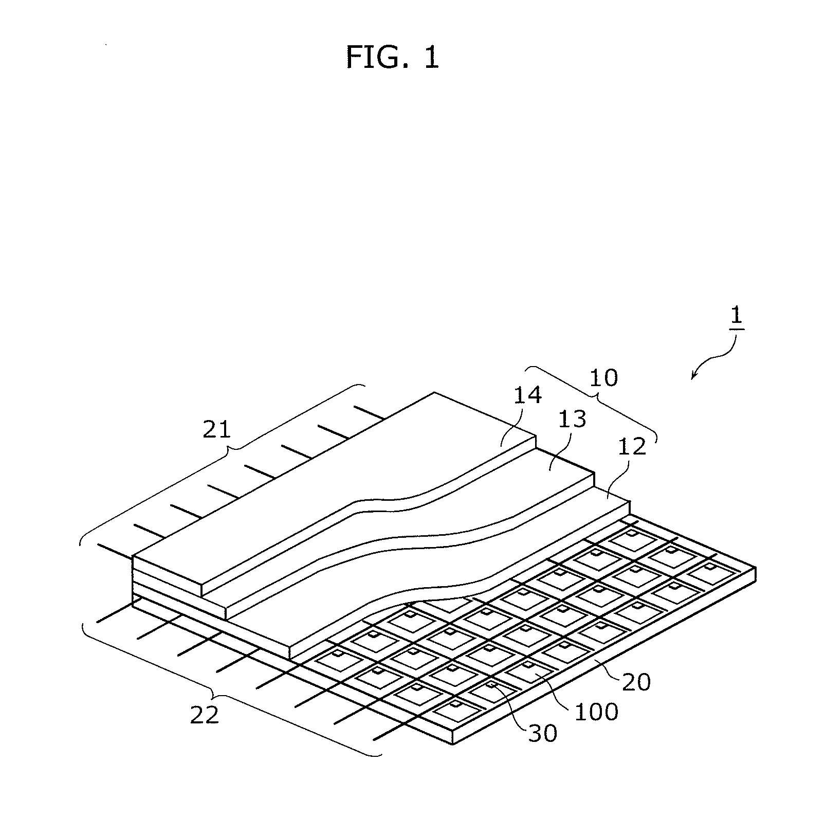
[0099]First, the organic electro-luminescence (EL) panel according to the first embodiment shall be described with reference to FIG. 1. FIG. 1 is a partial cutout perspective view of an organic EL display panel according to the first embodiment.

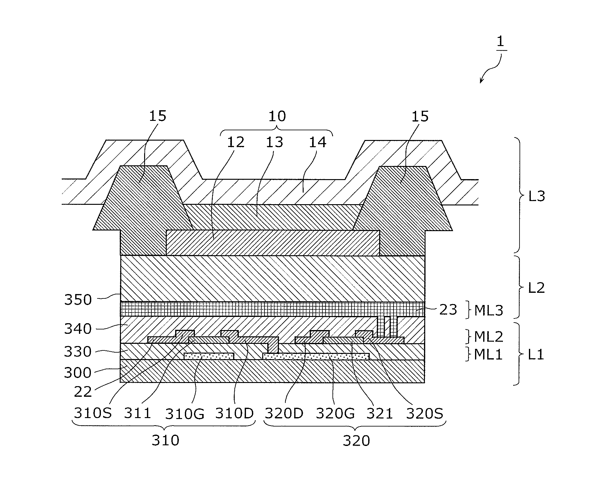
[0100]As illustrated in FIG. 1, the EL display panel 1 according to the first embodiment is an organic EL display panel (organic EL display), and includes an organic EL device 10 which is a light-emitting display device, and a thin-film semiconductor array device for display apparatus 20 composed of an active matrix substrate on which a thin-film transistor and lines are formed.

[0101]The organic EL device 10 includes lower electrodes 12, an organic light-emitting layer 13, and an upper electrode 14 that are sequentially formed on the thin-film semiconductor array device for display apparatus 20. The organic light-emitting layer 13 is composed of an electron transport layer, a light-emitting layer, a hole transport layer, and others stacked.

[0...

second embodiment

[0211]Next, the thin-film semiconductor device for display apparatus 3 according to the second embodiment shall be described with reference to FIGS. 14 to 16. FIG. 14 is a plan view of the thin-film semiconductor device for display apparatus according to the second embodiment. FIG. 15 is a plan view of the thin-film semiconductor device for display apparatus according to the second embodiment seeing through the lines and the insulating film formed in the line layer L2. FIG. 16 is a cross sectional view along X2-X2′ in FIG. 14. Note that, the cross sectional surface along X1-X1′ in FIG. 14 is identical to FIG. 9A.

[0212]The thin-film semiconductor device for display apparatus 3 according to the second embodiment has the same basic configuration as the thin-film semiconductor device for display apparatus 2 according to the first embodiment. Accordingly, in FIGS. 14 to 16, the same reference numerals are assigned to the components identical to the components illustrated in FIGS. 7 to 9B...

example 1

[0236]Next, an example of organic EL display panel in which thin-film semiconductor device for display apparatus according to the embodiments is used shall be described with reference to FIGS. 19A and 19B. FIG. 19A is a cross-sectional perspective view of an example of the organic EL display panel according to the present disclosure. FIG. 19B is a cross-sectional perspective view of an example of the organic EL display panel according to the present disclosure.

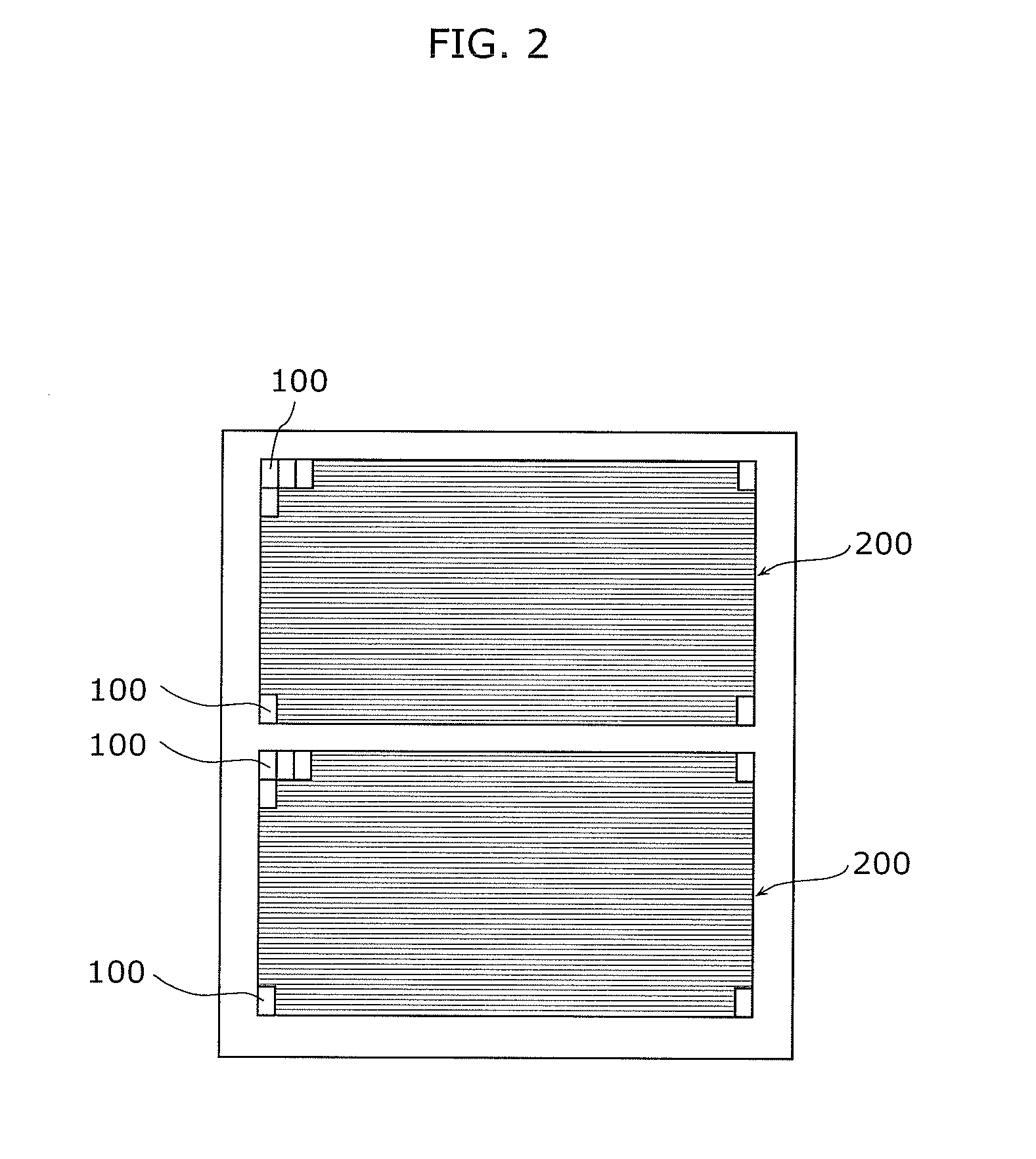
[0237]As illustrated in FIGS. 19A and 19B, the pixels 100 of the organic EL display panel include sub-pixels 100R, 100G, and 100B in three colors (red, green, and blue). Multiple sub-pixels 100R, 100G, and 100B are arranged in a depth direction of the FIGS. 19A and 19B (referred to as sub-pixel columns).

[0238]FIG. 19A illustrates an example of line banks, and the sub-pixel columns are separated by the banks 15. Each of the banks 15 illustrated in FIG. 19A includes a protrusion extending between the adjacent sub-pixel columns i...


PUM


Abstract

A thin-film semiconductor device for a display apparatus according to the present disclosure includes: a gate electrode above a substrate; a gate insulating film above the gate electrode; a semiconductor layer on the gate insulating film; a first electrode above the semiconductor layer; a second electrode in a same layer as the first electrode; an interlayer insulating film covering the first electrode and the second electrode; a gate line above the interlayer insulating film; and a power supply line in a same layer as the gate line and adjacent to the gate line. Furthermore, the gate electrode and the gate line are electrically connected via a first conductive portion, and the second electrode and the power supply line are electrically connected via a second conductive portion.

Description

CROSS REFERENCE TO RELATED APPLICATION[0001]This is a continuation application of PCT Patent Application No. PCT / JP2010 / 005845 filed on Sep. 29, 2010, designating the[0002]United States of America. The entire disclosures of the above-identified application, including the specification, drawings and claims are incorporated herein by reference in their entirety.TECHNICAL FIELD[0003]One or more exemplary embodiments disclosed herein relate generally to thin-film semiconductor devices for display apparatuses, methods for manufacturing thin-film semiconductor devices for display apparatuses, electro-luminescence (EL) display panels, and EL display apparatuses, and particularly relates to a thin-film semiconductor device for display apparatus used for an active-matrix display apparatus, and a method for manufacturing the thin-film semiconductor device for display apparatus.BACKGROUND ART[0004]Thin-film transistors (TFT) are used as a switching device for selecting pixel or a driving devic...

Claims


Application Information

Patent Timeline
IPC IPC(8): H01L33/36
CPCH01L27/124H01L33/387H01L33/36
Inventor KANEGAE, ARINOBU
Owner JOLED INC
Why Eureka
Try Eureka