Eureka AIR delivers breakthrough ideas for toughest innovation challenges, trusted by R&D personnel around the world.

Sensor array with high linearity

a sensor array and linear technology, applied in the field of large-area sensor arrays, can solve the problems of high power loss, limit the speed at which sampling operation may be performed, and high power consumption, and achieve the effects of reducing the dependence on the parasitic resistance of the signal address line, reducing power consumption, and stable bias voltag

Inactive Publication Date: 2013-04-04
SHARP KK
View PDF5 Cites 62 Cited by
  • Summary
  • Abstract
  • Description
  • Claims
  • Application Information

AI Technical Summary

Benefits of technology

The invention provides a way to read signals from active pixel sensor arrays using a current-mode readout method while accounting for non-linear behavior. This is achieved by incorporating the resistance of signal lines inside the current conveyor circuit, which helps to maintain a stable bias voltage across the pixel amplifier transistor. As a result, the read-out circuit is less affected by the resistance of the signal address lines and provides a more accurate measurement of the physical property being measured by the array.

Problems solved by technology

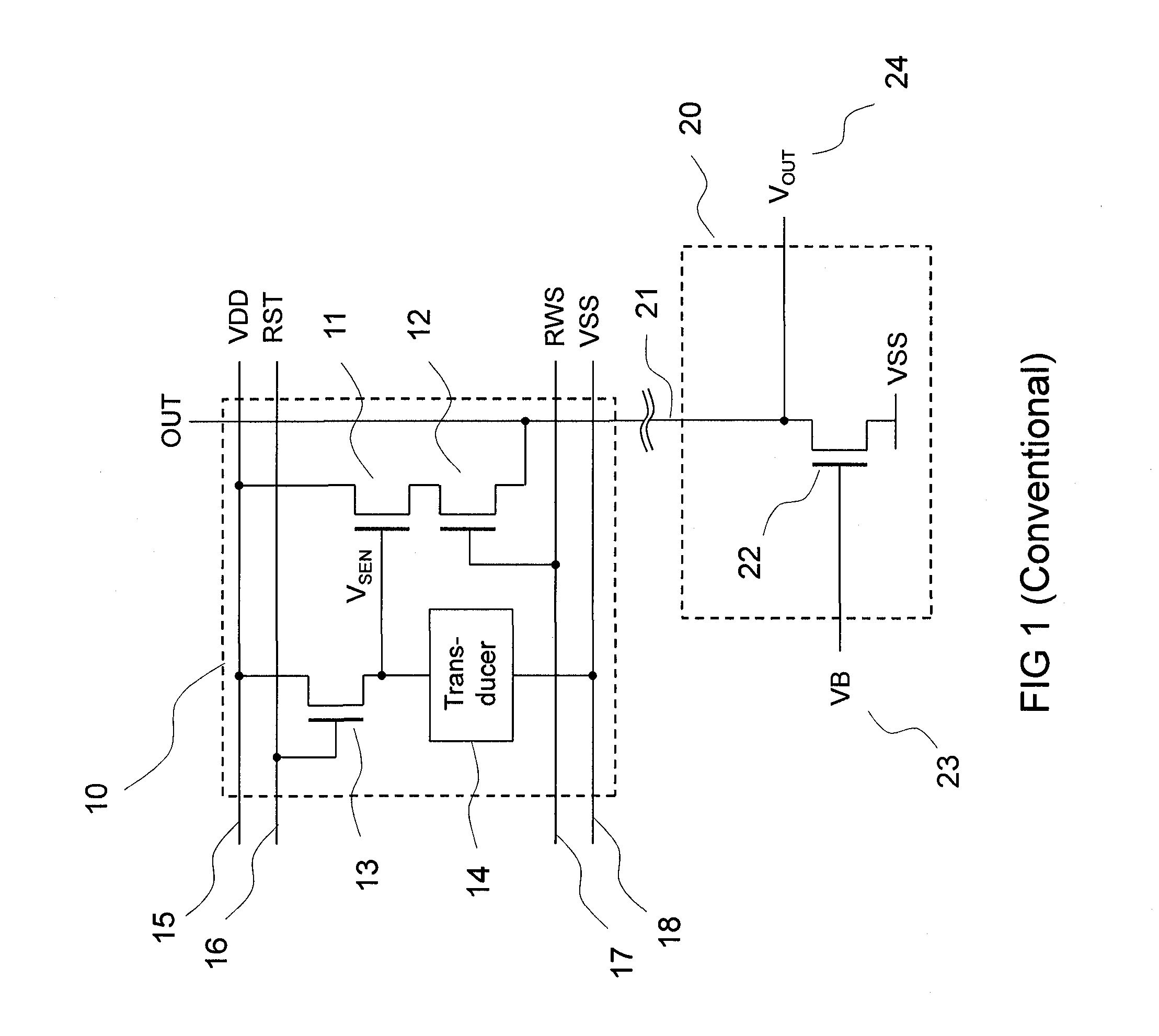
This results in a high power consumption since the entire parasitic capacitance of the address line (RWS) 17 must be charged during the sampling operation.
The process of charging and discharging this source line at high frequency results in high power losses and, due to the finite resistance of the output signal line 21, also places a limit on the speed at which the sampling operation may be performed.
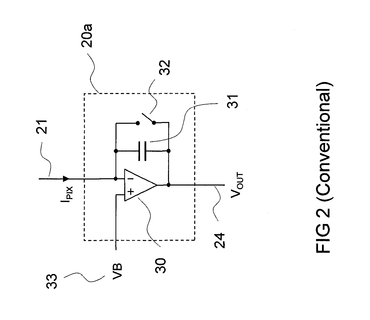
A disadvantage of using a single operational amplifier 30 to both bias the signal line 21 and perform current integration however is the high bandwidth requirement of the operational amplifier 30.
In practice, a non-ideal operational amplifier does not exhibit infinite bandwidth and may therefore be unable to sustain accurate voltage at its negative input terminal during the periods when the output voltage of the operational amplifier 30 changes quickly.
Whilst it is possible to provide an operational amplifier with sufficiently high bandwidth, such amplifiers typically exhibit high power consumption and require expensive, non-standard processing techniques to manufacture.
A disadvantage common to known current-mode type read-out circuits however is that in practice they exhibit lower input-to-output linearity than voltage-mode type read-out circuits.

Method used


Image

  • Sensor array with high linearity
  • Sensor array with high linearity
  • Sensor array with high linearity

Examples


first embodiment

[0222]The operation cycle of a one-transistor active pixel sensor circuit 300 is well-known and is now described only in summary. In a manner similar to the operation of the active pixel sensor circuit 110 of the first embodiment, during the first and second stage of the operation cycle (Periods 1 and 2) the active pixel sensor circuit 110 is reset and the physical signal to be measured is converted into a voltage signal, VSEN. Then, in the third and fourth stage of operation (Periods 3 and 4), the voltage signal generated in the pixel is sampled by the read-out circuit 200. The additional select addressing line (SEL) 313, provided by the control apparatus 240, may share similar timing with the row select line (RWS) 312 such that during Periods 3 and 4 the selection transistor 302 is turned on and a conductive path is formed between the reference voltage address line (VB1) 311 and the low potential power supply in the read-out circuit 200 (via the pixel amplifier transistor 301, pix...

third embodiment

[0224]In this invention, the current conveyor circuit 210 of the previous embodiments is replaced with an alternative form of current conveyor circuit that makes use of a current mirror formed by p-type transistors. This p-type current conveyor circuit 340 is shown in the schematic diagram of FIG. 9 and includes an operational amplifier 341 an input p-type transistor 342 and an output p-type transistor 343. The input and output transistors are well matched and form a current mirror. The source terminals of the p-type transistors 342,343 are connected to a high potential power supply (VDD), while their gate terminals are connected together and to the output of the operational amplifier 341. The drain terminal of the input transistor 342 is connected to the source drive addressing line 131 and the drain terminal of the output transistor 343 to the input of a current integrator circuit 220 of the type shown in FIG. 5, for example. The source sense addressing line 132 is connected to th...

fourth embodiment

[0225]In this invention, the current conveyor circuit of the previous embodiments is formed by a combination of n-type and p-type current mirrors. As shown in FIG. 10, this current conveyor circuit 360 includes an operational amplifier 361 and two branches, an input bias branch 362 and output bias branch 363. The input bias branch 362 includes a p-type transistor 370 and two n-type transistors 371, 372 connected in series between the high and low potential power supplies (VDD and VSS respectively). Similarly, the output bias branch 363 includes a p-type transistor 375 and two n-type transistors 376, 377 connected in series between the high and low potential power supplies (VDD and VSS respectively). The p-type transistor 370 of the input bias branch 362 and the p-type transistor 375 of the output bias branch 363 are well-matched and form a first p-type current mirror with a bias voltage (VB3) 373 supplied externally. The n-type transistor 372 of the input bias branch 362 and the n-t...


PUM


Abstract

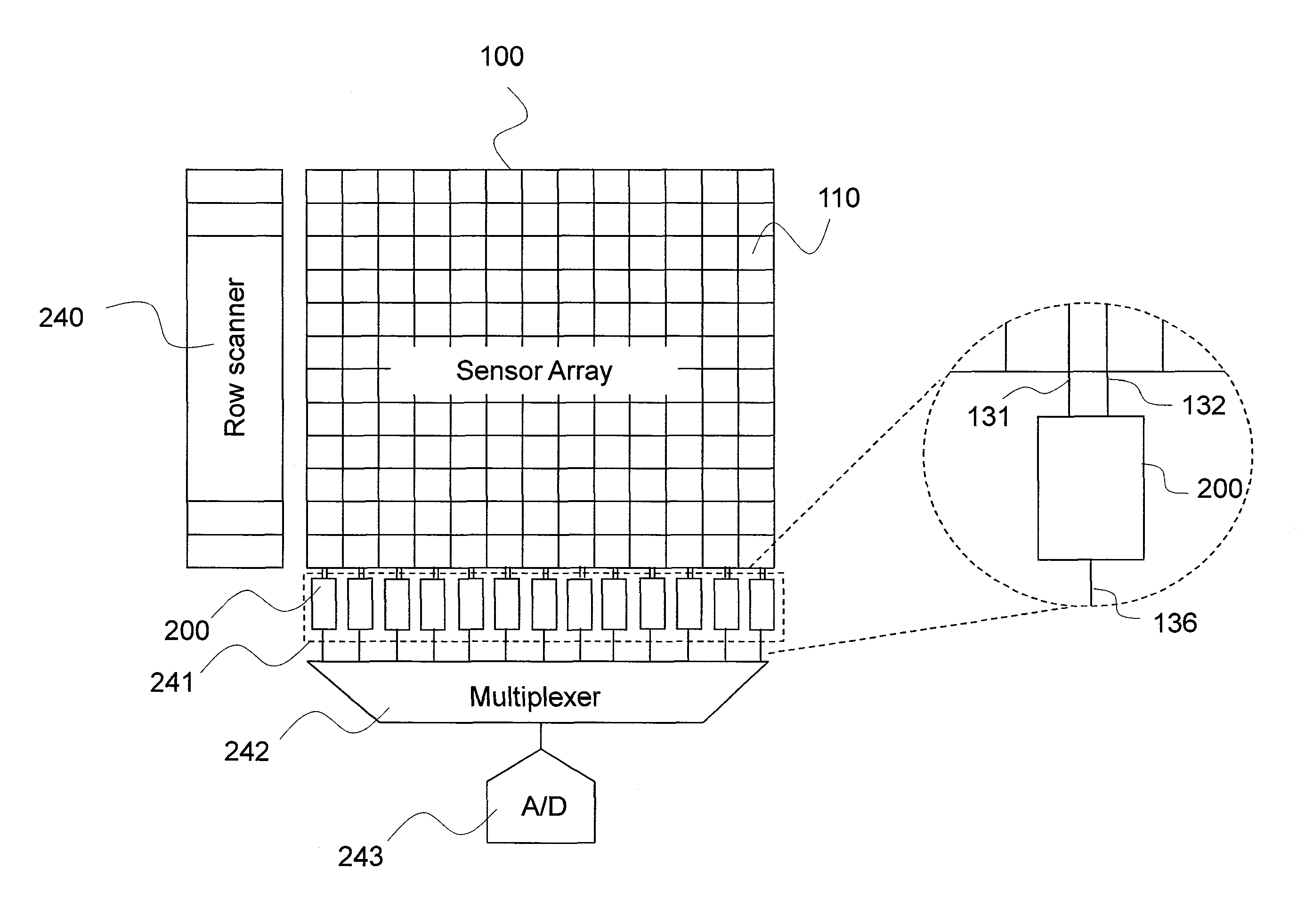
A sensor array includes a plurality of pixel sensor circuits; and a current-mode readout circuit to sample signals generated in each pixel sensor circuit; and addressing circuitry to individually select each pixel sensor circuit. Each pixel sensor circuit includes: a transducer and an amplifying element coupled to the transducer and configured to output a signal current which varies as a function of a measured physical property. The current-mode readout circuit includes: a sense signal line coupled to each of the amplifying elements in order to monitor the voltage presented across the amplifying element of the selected pixel sensor circuit; a drive signal line coupled to an output of each of the amplifying elements in order to provide a constant bias voltage to the amplifying element of the selected pixel sensor circuit; and a current conveyor circuit coupled to the sense signal line and drive signal line.

Description

TECHNICAL FIELD[0001]The invention belongs in the field of large area sensor arrays. More specifically, the invention can be used to improve the performance of a class of sensor array readout circuits known as current-mode readout circuits. The invention is particularly relevant to sensor arrays with high address line resistances as occurs, for example, when the array is of a large physical size or when the process technology used in the fabrication of the array limits the conductivity of the material that can be used to create the address line.[0002]This invention finds application in different types of sensor arrays such as, but not limited to, image sensor arrays, chemical sensor arrays and touch panels including touch panels integrated within liquid crystal display (LCD) devices.BACKGROUND ART[0003]Sensor arrays are formed by a plurality of sensor pixels wherein each pixel contains a transducer to convert some physical property—such as, but not limited to, light, temperature, pr...

Claims


Application Information

Patent Timeline
Patent Type & Authority Applications(United States)
IPC IPC(8): G06F3/041H01L27/146G01J1/42
CPCH04N5/378H01L27/14609H04N25/78H04N25/77H04N25/75
Inventor ISLAMKULOV, DAURENCASTILLO, SERGIO GARCIABROWN, CHRISTOPHER JAMES
Owner SHARP KK
Why Eureka
Eureka Blog
Learn More