
RF pulse signal generation switching circuit, RF pulse signal generating circuit, and target object detecting apparatus

a technology of pulse signal generation and switching circuit, which is applied in the direction of pulse technique, gated amplifier, instruments, etc., can solve the problems of low stability in operation, long fall time length of general operational amplifier, so as to improve the accuracy of target object detection at a distance, reduce the noise generated immediately after the switch from a transmission period to a reception period, and improve the effect of receiving sensitivity

Active Publication Date: 2013-04-11
FURUNO ELECTRIC CO LTD
View PDF22 Cites 14 Cited by
  • Summary
  • Abstract
  • Description
  • Claims
  • Application Information

AI Technical Summary

Benefits of technology

The present patent text describes a configuration for improving the detection of target objects in a close distance by using a stable RF pulse signal with a rapid pulse fall. This is achieved by providing an RF pulse signal generating circuit to the transmitter and shifting from ON to OFF of the supply of the drive voltage to the drain of the power FET quickly. This results in a reduction of transmission noise and improves the receiving sensitivity, accordingly.

Problems solved by technology

However, with the method of controlling the gate voltage of the power FET, although an operational amplifier is generally used, a fall time length of the general operational amplifier is long.
Further, with an operational amplifier with high unity gain frequency (ft), although the fall time length is shorter, there is a problem of output waveform ringing, and stability in operation being LOW.
However, the FET 212P used as a high-side FET is a p-type FET of which an input capacity is large and a responding speed of falling is slow.

Method used


Image

  • RF pulse signal generation switching circuit, RF pulse signal generating circuit, and target object detecting apparatus
  • RF pulse signal generation switching circuit, RF pulse signal generating circuit, and target object detecting apparatus
  • RF pulse signal generation switching circuit, RF pulse signal generating circuit, and target object detecting apparatus

Examples


Embodiment Construction

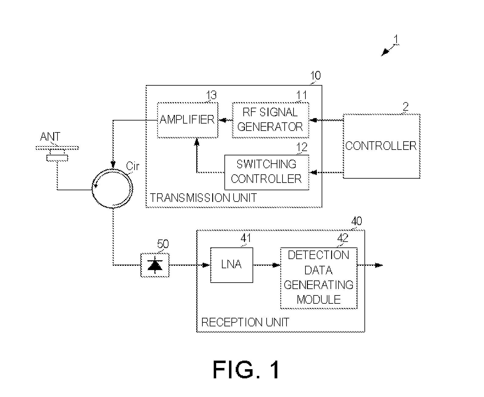
[0033]An RF pulse signal generation switching circuit, an RF pulse signal generating circuit, and a target object detecting apparatus according to an embodiment of the invention are described with reference to the appended drawings. Note that, in this embodiment, the target object detecting apparatus is described by using a radar apparatus as an example. However, the configuration of the present invention can be applied to other apparatuses that use a pulse-wave shaped RF signal as a transmission signal (e.g., sonar apparatuses and school-of-fish detecting apparatuses).

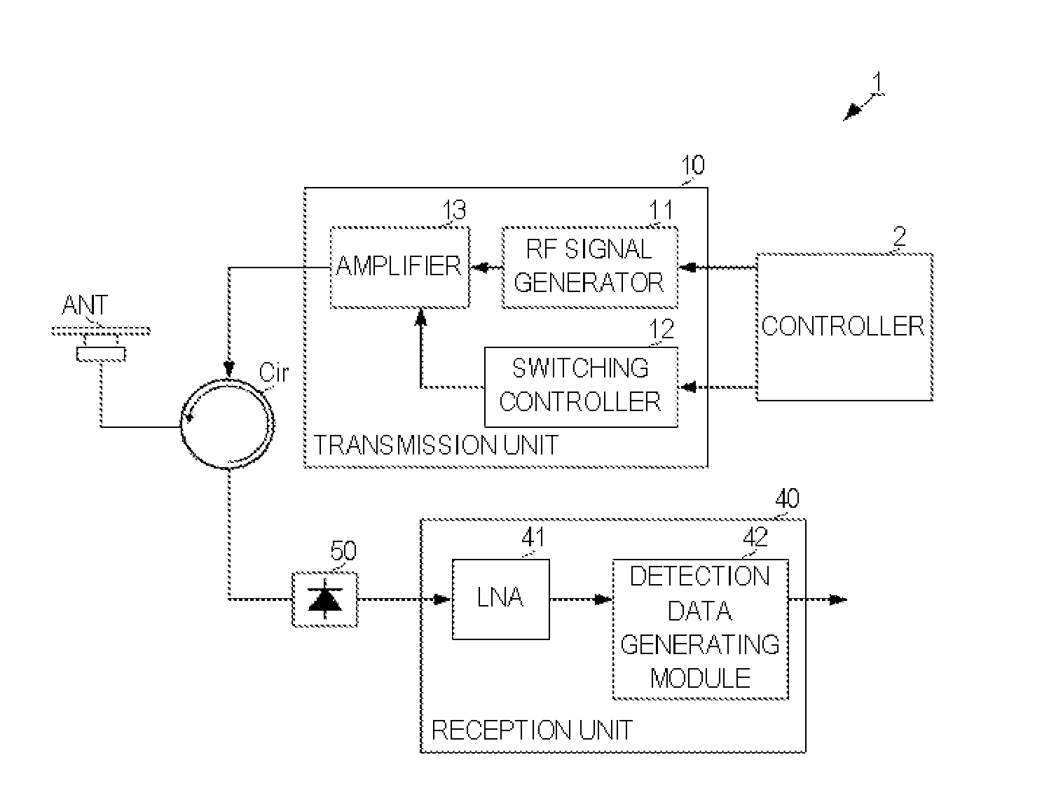
[0034]FIG. 1 is a block diagram illustrating a main configuration of a radar apparatus 1 according to this embodiment. The radar apparatus 1 includes a controller 2, a transmission unit 10 (corresponding to the “RF pulse signal generating circuit” in the claims), a reception unit 40, a limiter 50, a circulator Cir, and an antenna ANT.

[0035]The controller 2 performs an overall control, such as a power control, of the r...


PUM


Abstract

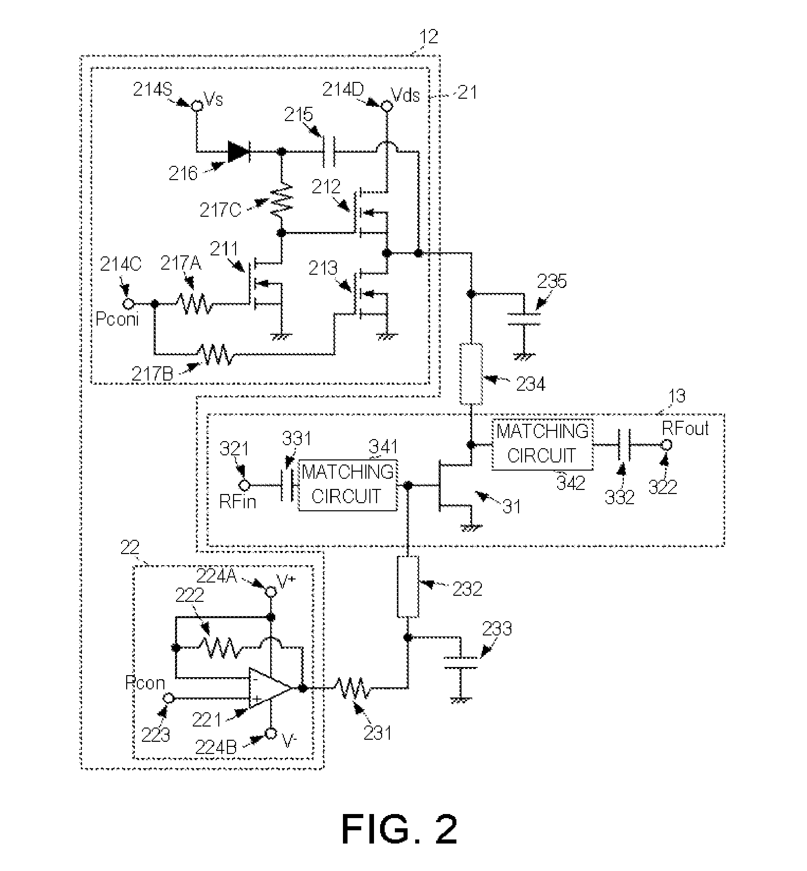
An RF pulse signal generation switching circuit for controlling an output of a power FET for amplifying a high frequency signal to generate an RF pulse signal that is the high frequency signal pulse formed into a pulse-wave shape is provided. The circuit includes first and third n-type FETs of which gates are inputted with a control pulse that supplies a rise timing and a fall timing of a pulse, and a second n-type FET of which a gate is connected with a drain of the first FET. A source of the first FET and a source of the third FET are grounded, respectively. The drain of the first FET is applied with a first drive voltage via a resistor. A drain of the second FET is applied with a second drive voltage. A source of the second FET is connected with a drain of the third FET and the connection point therebetween is connected with the power FET. A capacitor is connected between the connection point and an end of the resistor from which the first drive voltage is applied.

Description

CROSS-REFERENCE TO RELATED APPLICATION(S)[0001]The application claims priority under 35 U.S.C. §119 to Japanese Patent Application No. 2011-223570, which was filed on Oct. 11, 2011, the entire disclosure of which is hereby incorporated by reference.TECHNICAL FIELD[0002]The present invention relates to an RF pulse signal generating circuit for generating a pulse transmission signal that is used in a target object detecting apparatus such as a radar apparatus, and a switching circuit used in the generating circuit.BACKGROUND OF THE INVENTION[0003]Conventionally, target object detecting apparatuses, such as radar apparatuses, have been performing detections of target objects by transmitting high frequency signals (RF signals) to detection ranges and receiving reflection signals that are the transmission signals respectively reflected on the target objects.[0004]JP4081035B discloses a target object detecting apparatus that forms an RF signal into a pulse-wave shape and transmits the RF ...

Claims


Application Information

Patent Timeline
Patent Type & Authority Applications(United States)
IPC IPC(8): G01S13/04H03K3/012
CPCG01S7/282H03K17/063H03F1/0261H03F1/56H03F3/193H03F3/245H03F2200/15H03F2200/18H03F2200/21H03F2200/222H03F2200/27H03F2200/387H03F2200/555H03F2203/7203G01S7/03H03K17/04163H03F3/72
Inventor KOBAYASHI, TOMONAO
Owner FURUNO ELECTRIC CO LTD
Learn More