

Semiconductor device and method for manufacturing the same
a semiconductor and semiconductor technology, applied in the direction of transistors, electroluminescent light sources, electric lighting sources, etc., can solve the problems of shape defects or degradation of electric characteristics, and achieve the effect of improving reliability, reducing resistance, and reducing resistan
- Summary
- Abstract
- Description
- Claims
- Application Information
AI Technical Summary
Benefits of technology
Problems solved by technology
Method used
Image

Examples
embodiment 1
[0045]In this embodiment, an embodiment of a semiconductor device and a manufacturing method thereof will be described with reference to FIGS. 1A to 1C, FIGS. 2A to 2E, FIGS. 3A to 3C, FIGS. 4A to 4C, and FIGS. 5A to 5C. In this embodiment, a transistor including an oxide semiconductor film will be described as an example of the semiconductor device.
[0046]The transistor may have a single-gate structure in which one channel formation region is formed, a double-gate structure in which two channel formation regions are formed, or a triple-gate structure in which three channel formation regions are formed. Alternatively, the transistor may have a dual-gate structure including two gate electrode layers positioned above and below a channel formation region with a gate insulating film provided therebetween.
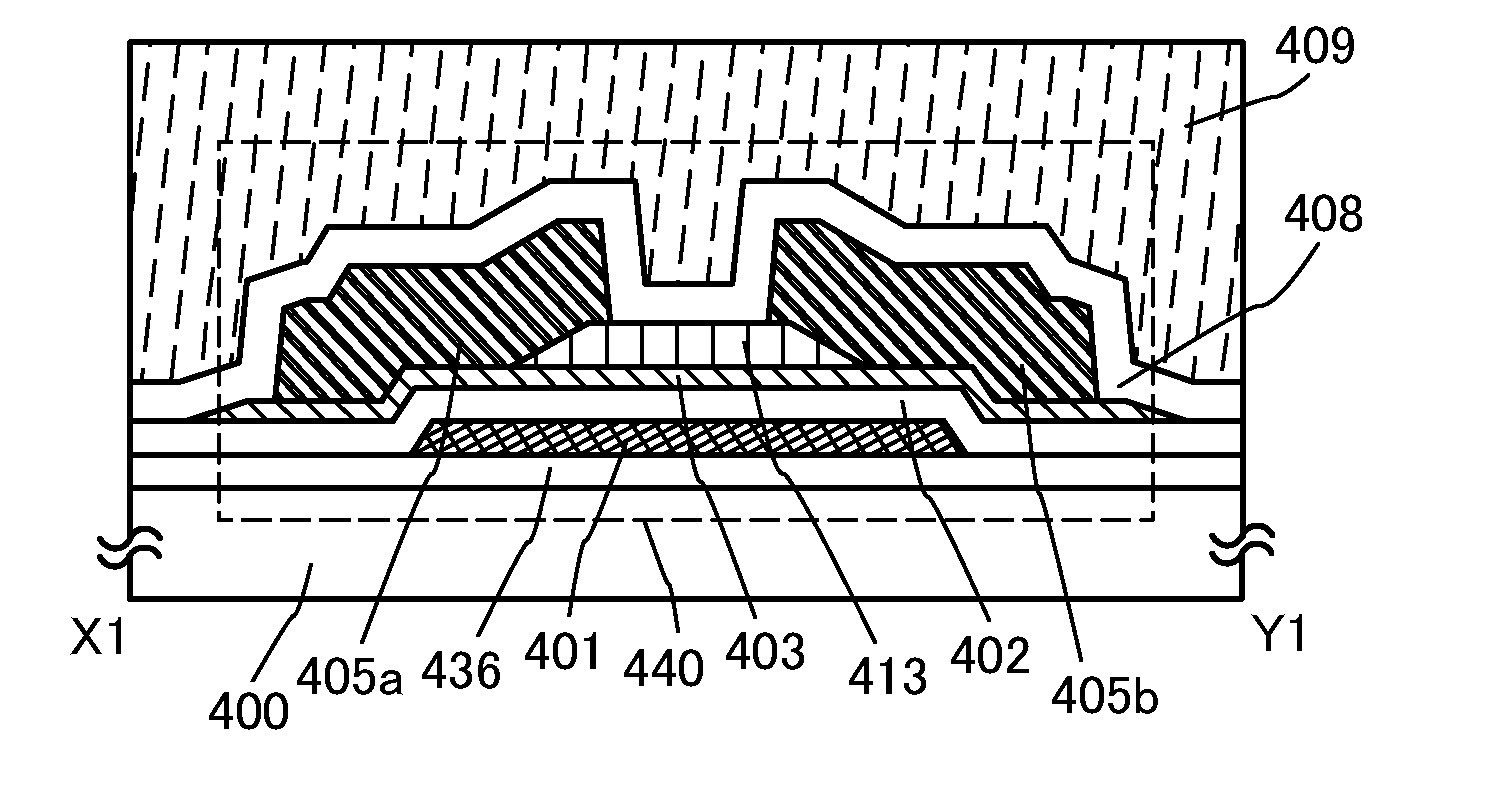
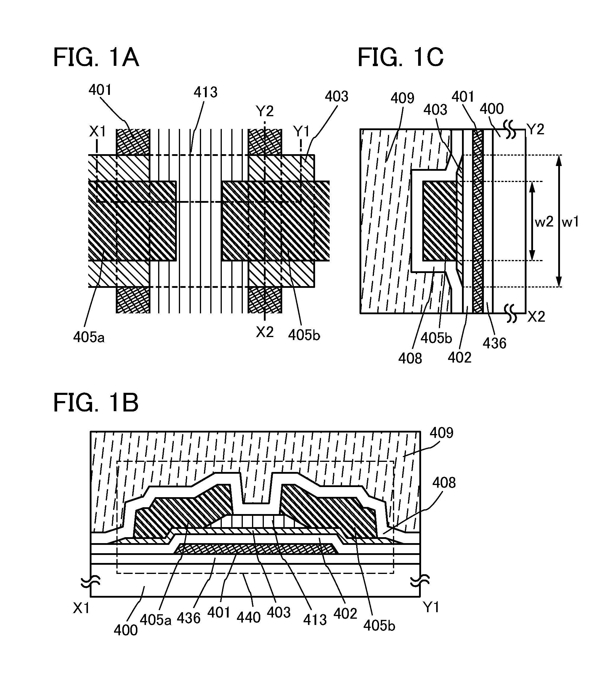
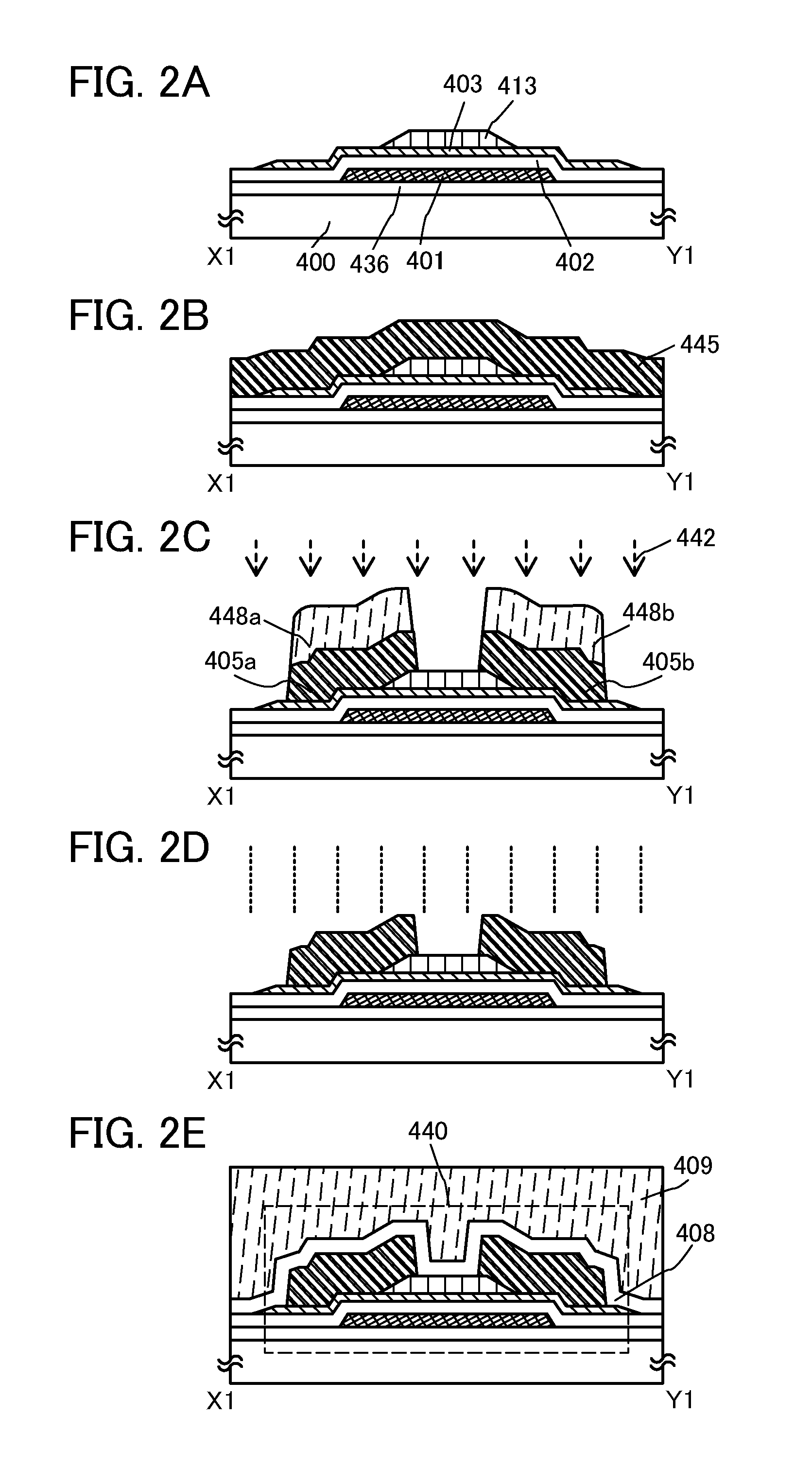
[0047]A transistor 440 illustrated in FIGS. 1A to 1C is an example of a transistor which is one of bottom-gate transistors and is also referred to as an inverted staggered transistor. FI...
embodiment 2
[0179]In this embodiment, one embodiment of a semiconductor device and one embodiment of a method for manufacturing the semiconductor device which are different from those in Embodiment 1 will be described using FIGS. 6A to 6C, FIGS. 7A to 7E, and FIGS. 8A to 8C. In this embodiment, a transistor including an oxide semiconductor film will be described as an example of the semiconductor device.
[0180]The transistor may have a single-gate structure in which one channel formation region is formed, a double-gate structure in which two channel formation regions are formed, or a triple-gate structure in which three channel formation regions are formed. Alternatively, the transistor may have a dual-gate structure including two gate electrode layers positioned above and below a channel formation region with a gate insulating film provided therebetween.
[0181]A transistor 480 illustrated in FIGS. 6A to 6C is an example of a transistor which is one of bottom-gate transistors and is also referred...
embodiment 3
[0217]A semiconductor device having a display function (also referred to as a display device) can be manufactured using the transistor described in Embodiment 1 or 2. Some or all of driver circuits including transistors can be formed over a substrate where a pixel portion is formed, whereby a system-on-panel can be obtained.
[0218]In FIG. 9A, a sealant 4005 is provided so as to surround a pixel portion 4002 provided over a first substrate 4001, and the pixel portion 4002 is sealed by using a second substrate 4006. In FIG. 9A, a signal line driver circuit 4003 and a scan line driver circuit 4004 which are each formed using a single crystal semiconductor film or a polycrystalline semiconductor film over a substrate separately prepared are mounted in a region that is different from the region surrounded by the sealant 4005 over the first substrate 4001. Various signals and potential are supplied to the signal line driver circuit 4003 and the scan line driver circuit 4004 each of which i...
PUM
 Abstract
Description
Claims
Application Information