Electrostatic discharge protection device

a protection device and electrostatic discharge technology, applied in semiconductor devices, semiconductor/solid-state device details, electrical apparatus, etc., can solve the problems of increasing the leakage current of the device, reducing the protection capability of the electrostatic discharge (esd) of the integrated circuit, and the transistor often cannot be completely turned off, etc., to achieve the reduction of the rise time of the input signal, the effect of reducing the leakage current of the esd protection device and high operating speed

Inactive Publication Date: 2013-04-25
MACRONIX INT CO LTD
View PDF9 Cites 18 Cited by
  • Summary
  • Abstract
  • Description
  • Claims
  • Application Information

AI Technical Summary

Benefits of technology

[0016]According to the above descriptions, the NMOS transistor is not easy to be triggered due to a series structure of the NMOS transistor and the voltage-drop element. In this way, although the rising time of the input signal is shortened, the input signal coupled to the gate of the NMOS transistor is not easy to trigger the NMOS transistor. Therefore, the ESD protection device can be applied in an integrated circuit (IC) with a high operating speed, and leakage current in the ESD protection device can also be reduced.

Problems solved by technology

However, the above advanced process techniques may also result in reduction of an electrostatic discharge (ESD) protection capability of an integrated circuit (IC).
Therefore, to enhance the device ESD protection capability is an important issue to be developed in design of deep sub-micro devices.
However, in an actual application, when a rising time of the electrostatic signal come from the pad is shortened, the NMOS transistor often cannot be completely turned off, which may increase the leakage current of the device.
In other words, the existing gate-coupled ESD protection device cannot be applied in ICs with a high operating speed.

Method used


Image

  • Electrostatic discharge protection device
  • Electrostatic discharge protection device
  • Electrostatic discharge protection device

Examples


Embodiment Construction

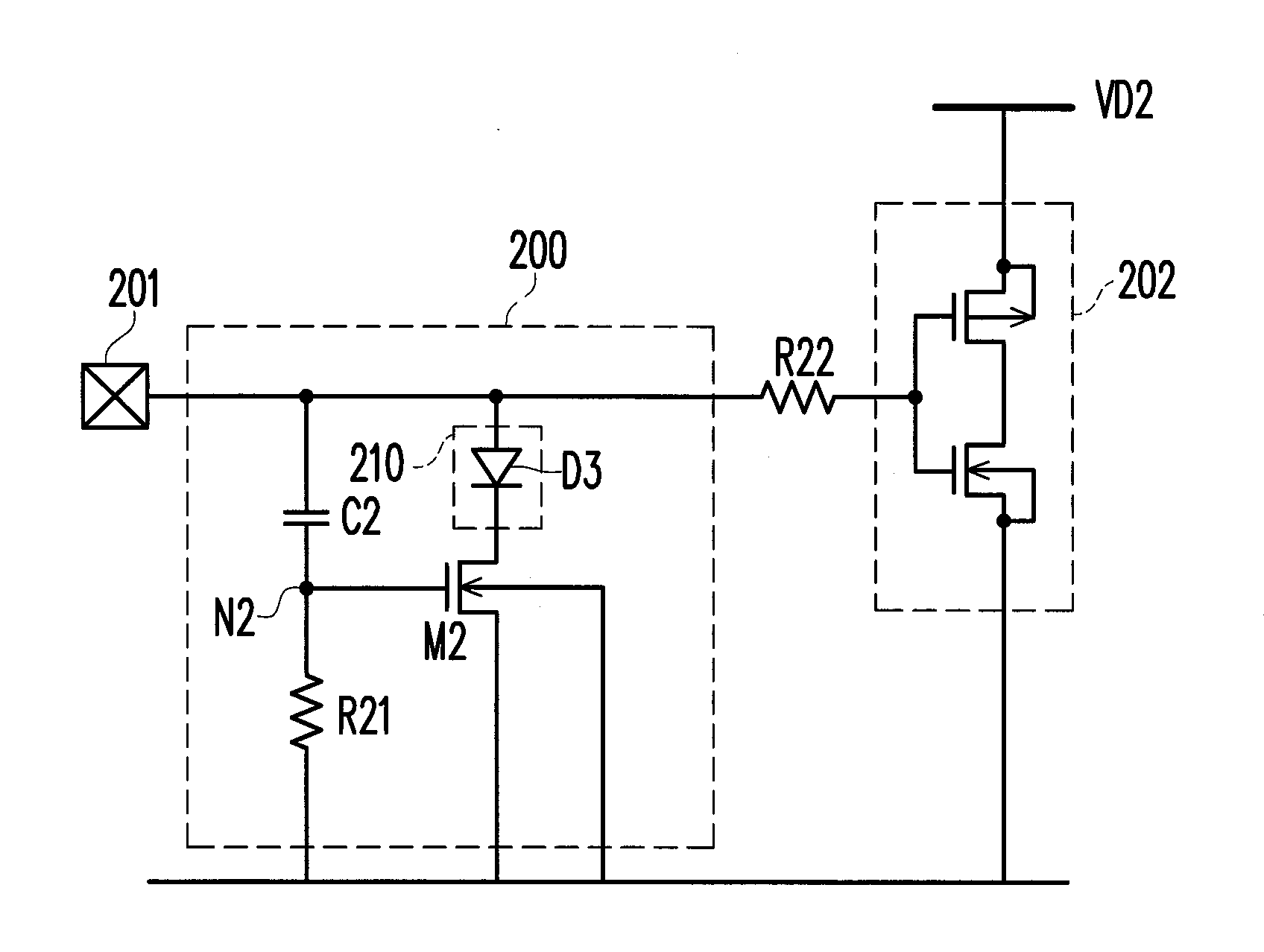
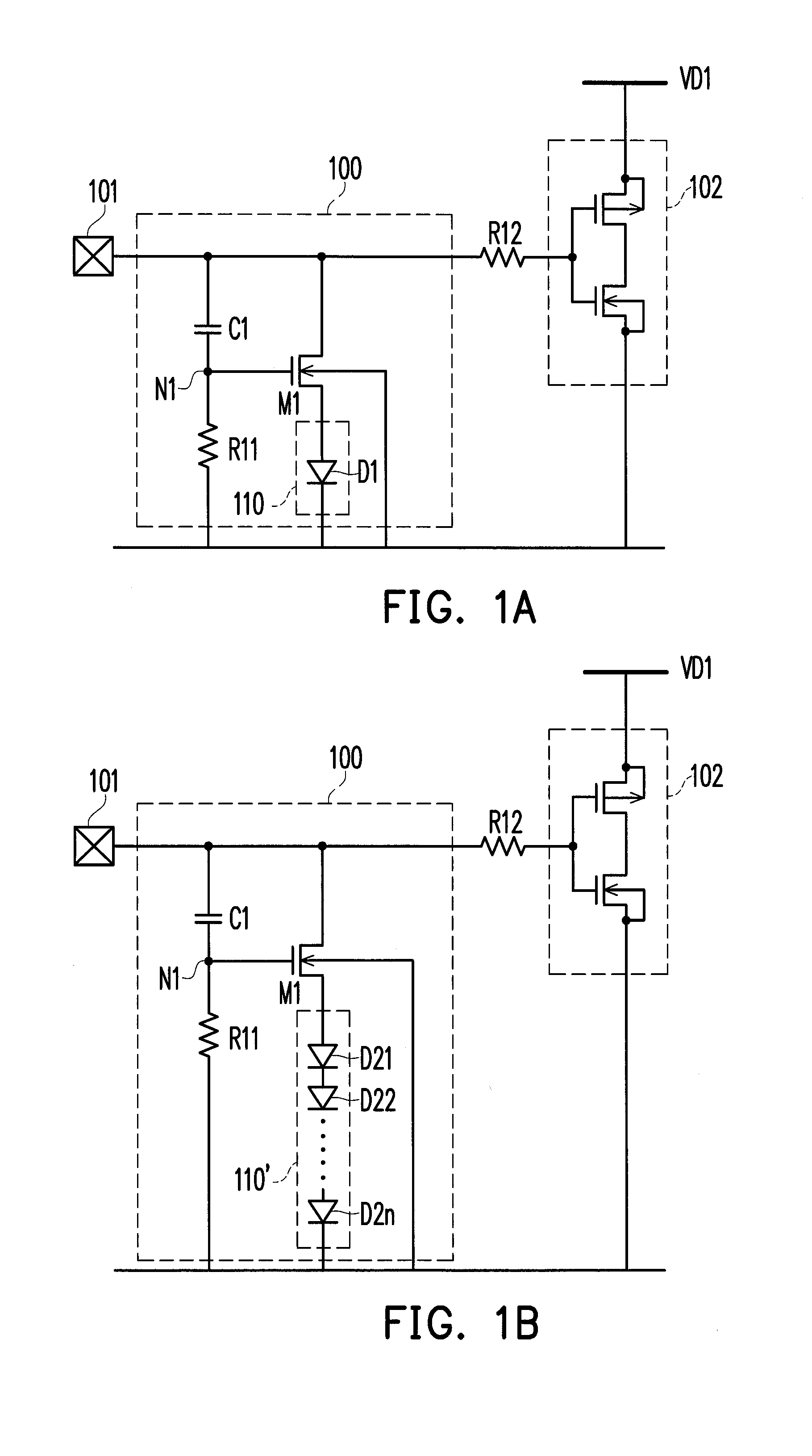
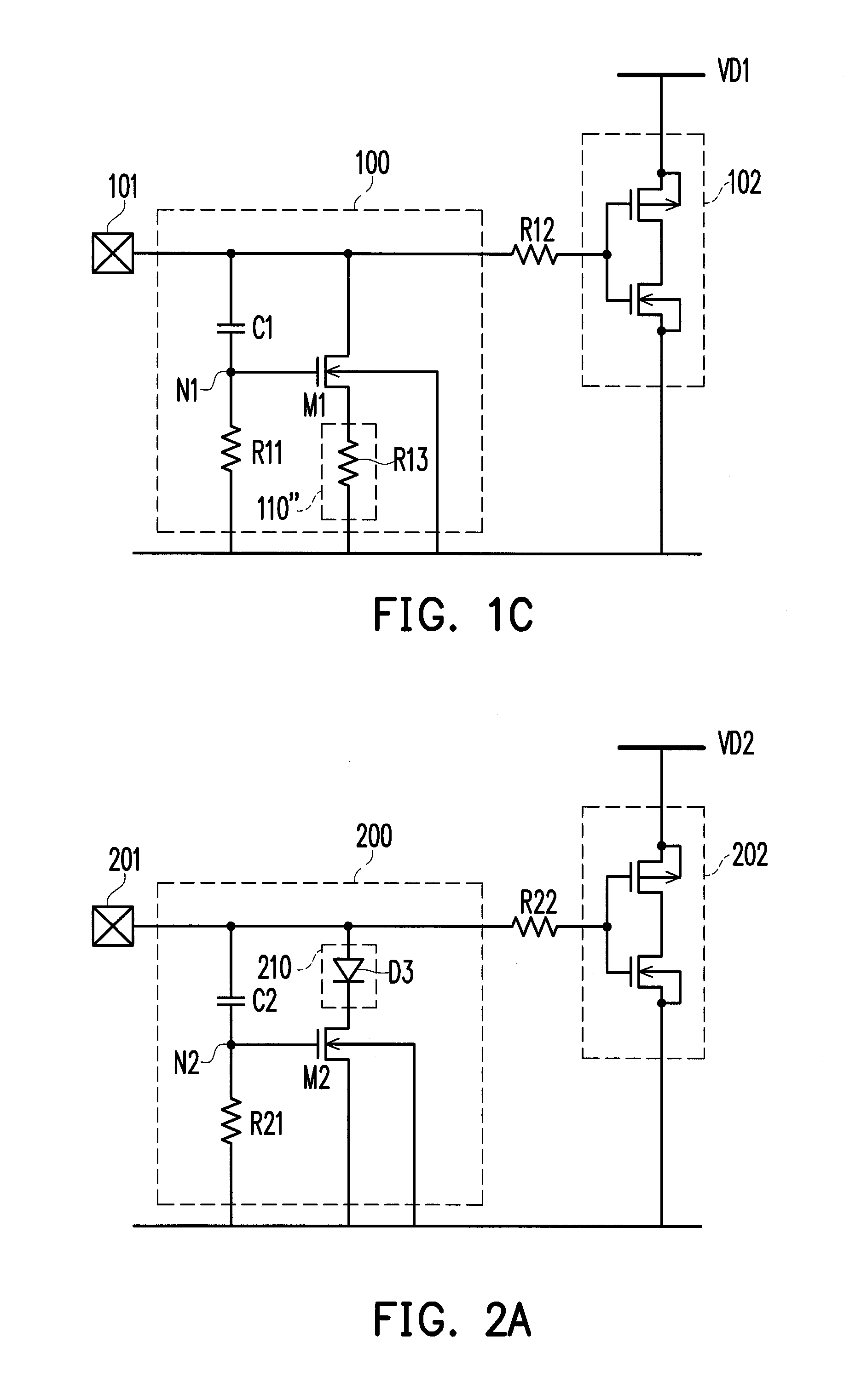
[0023]FIG. 1A is a circuit diagram of an electrostatic discharge (ESD) protection device according to an embodiment of the invention. Referring to FIG. 1A, the ESD protection device 100 is electrically connected to a pad 101 and is electrically connected to an internal circuit 102 through a resistor R12. The ESD protection device 100 is used to prevent an electrostatic signal of the pad 101 from damaging the internal circuit 102. When the internal circuit 102 normally operates, the internal circuit 102 is operated under a power voltage VD1, and receives an input signal through the pad 101.

[0024]The ESD protection device 100 includes a capacitor C1, a resistor R11, an N-channel metal oxide semiconductor (NMOS) transistor M1 and a voltage-drop element 110. The ESD protection device 100 is a gate-coupled ESD protection device, so that in view of an electrical connection, a first end of the capacitor C1 is electrically connected to the pad 101. Moreover, a first end of the resistor R11 ...


PUM


Abstract

An electrostatic discharge protection device electrically connected between a pad and an internal circuit is provided and includes a capacitor, a first resistor, a voltage-drop element and an NMOS transistor. A first end of the capacitor is electrically connected to the pad. A first end of the first resistor is electrically connected to a second end of the capacitor, and a second end of the first resistor is electrically connected to ground. The NMOS transistor and the voltage-drop element are connected in series between the pad and the ground, a gate of the NMOS transistor is electrically connected to the second end of the capacitor, and a bulk of the NMOS transistor is electrically connected to the ground.

Description

BACKGROUND OF THE INVENTION[0001]1. Field of the Invention[0002]The invention relates to an electrostatic discharge (ESD) protection device. Particularly, the invention relates to a gate-coupled ESD protection device.[0003]2. Description of Related Art[0004]As a complementary metal oxide semiconductor (CMOS) process enters a deep sub-micron scale, many advanced process techniques are used in order to reduce a device size and maintain device characteristics, for example, a relatively thin gate oxide layer, a relatively short channel length, a relatively shallow junction depth, a lightly-doped drain (LDD) structure, and a self-aligned silicide structure, etc. However, the above advanced process techniques may also result in reduction of an electrostatic discharge (ESD) protection capability of an integrated circuit (IC). Therefore, to enhance the device ESD protection capability is an important issue to be developed in design of deep sub-micro devices.[0005]Generally, the existing ICs...

Claims


Application Information

Patent Timeline
Patent Type & Authority Applications(United States)
IPC IPC(8): H01L27/092
CPCH01L27/0285
Inventor HE, CHIEH-WEIXU, QI-AN
Owner MACRONIX INT CO LTD
Why Eureka
Try Eureka