High selectivity nitride etch process

a nitride etching and selective etching technology, applied in the field of anisotropic can solve the problems of poor selectivity of a nitride etching process, difficult etching of silicon nitride to more than one material, and often observed poor selective etching performance of silicon nitride, and achieve the effect of low reaction ra

Active Publication Date: 2013-05-02
ZEON CORP +1
View PDF0 Cites 34 Cited by
  • Summary
  • Abstract
  • Description
  • Claims
  • Application Information

AI Technical Summary

Benefits of technology

[0007]An anisotropic silicon nitride etch provides selectivity to silicon and silicon oxide by forming a fluorohydrocarbon-containing polymer on silicon surfaces and silicon oxide surfaces. Selective fluorohydrocarbon deposition is employed to provide selectivity to non-nitride surfaces. The fluorohydrocarbon-containing polymer interacts with silicon nitride to form a volatile compound, thereby enabling etching of silicon nitride. The fl

Problems solved by technology

Etching silicon nitride selective to more than one material is very challenging.
Poor performance in selective etching of silicon nitride is often observed especially at the nanoscale level.
An example of poor performance in selectivity of a nitride etch process is observed in the spacer module in which silicon nitride spacers are formed to electrically isolate gate electrodes from source and drain regions.
Lack of sufficient selectivity causes formation of recesses within semiconductor material portions that are not covered by the gate electrodes.
Another example of poor performance in selectivity of a nitride etch is observed in a trench silicide etch in which a silicon nitride layer is emplo

Method used


Image

  • High selectivity nitride etch process
  • High selectivity nitride etch process
  • High selectivity nitride etch process

Examples


first embodiment

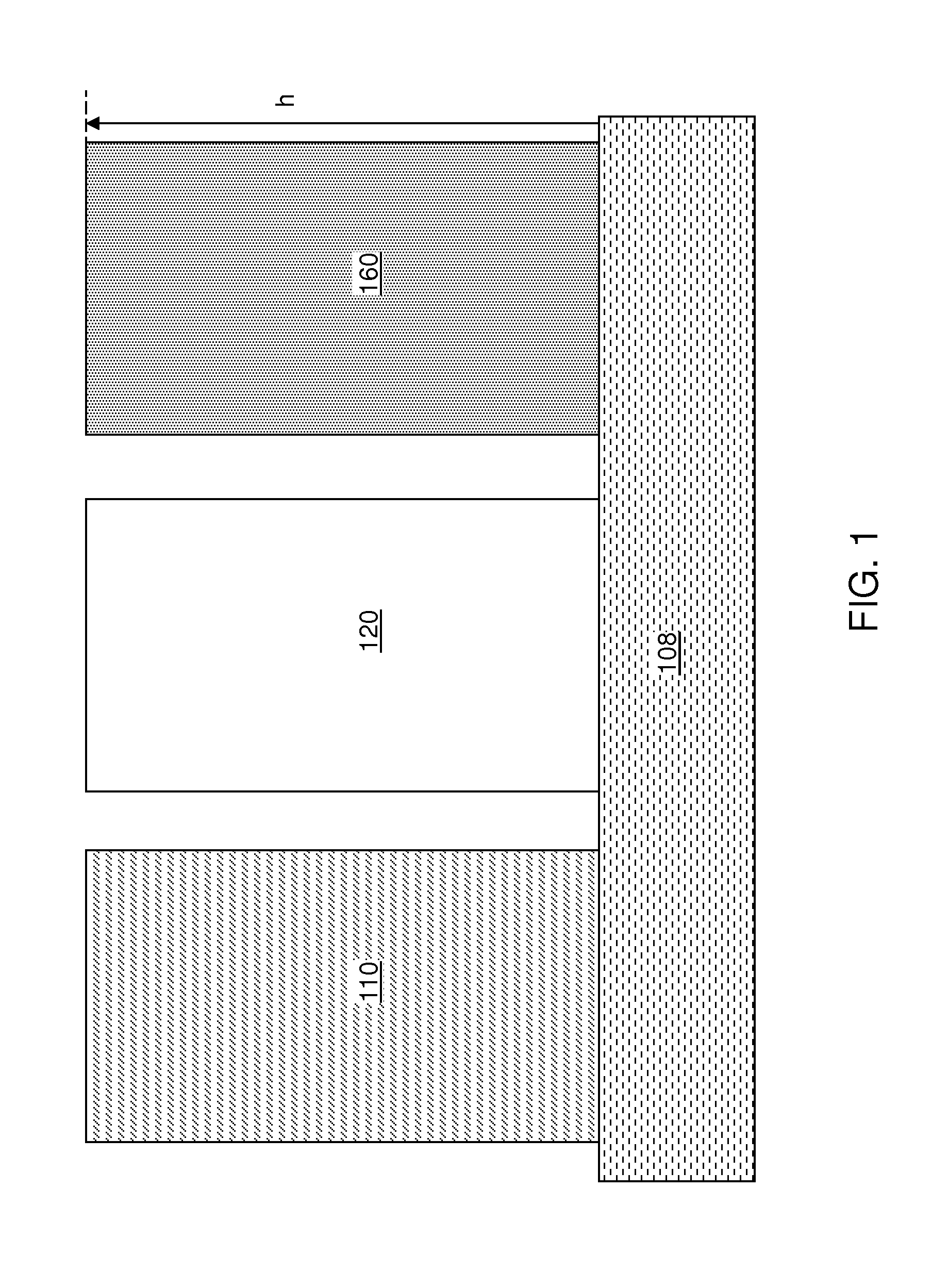
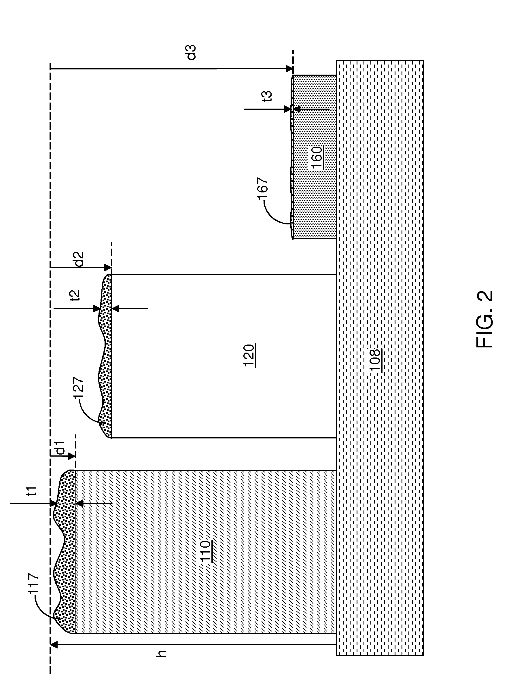
[0026]Referring to FIG. 1, a first exemplary structure according to the present disclosure includes a substrate 108, a silicon portion 110 located on a portion of a top surface of the substrate 108, a silicon oxide portion 120 located on another portion of the top surface of the substrate 108, and a silicon nitride portion located on yet another portion of the top surface of the substrate 108. The substrate 108 can include a semiconductor material such as single crystalline silicon, polysilicon, amorphous silicon, a silicon germanium alloy, a silicon carbon alloy, a silicon germanium carbon alloy, a III-V compound semiconductor material, a II-VI compound semiconductor material, or a combination thereof. Alternately or additionally, the substrate 108 can include an insulator material such as silicon oxide, doped derivatives of silicon oxide, silicon nitride, silicon oxynitride, a dielectric metal oxide having a dielectric constant greater than 3.9, or a combination thereof. Alternate...

second embodiment

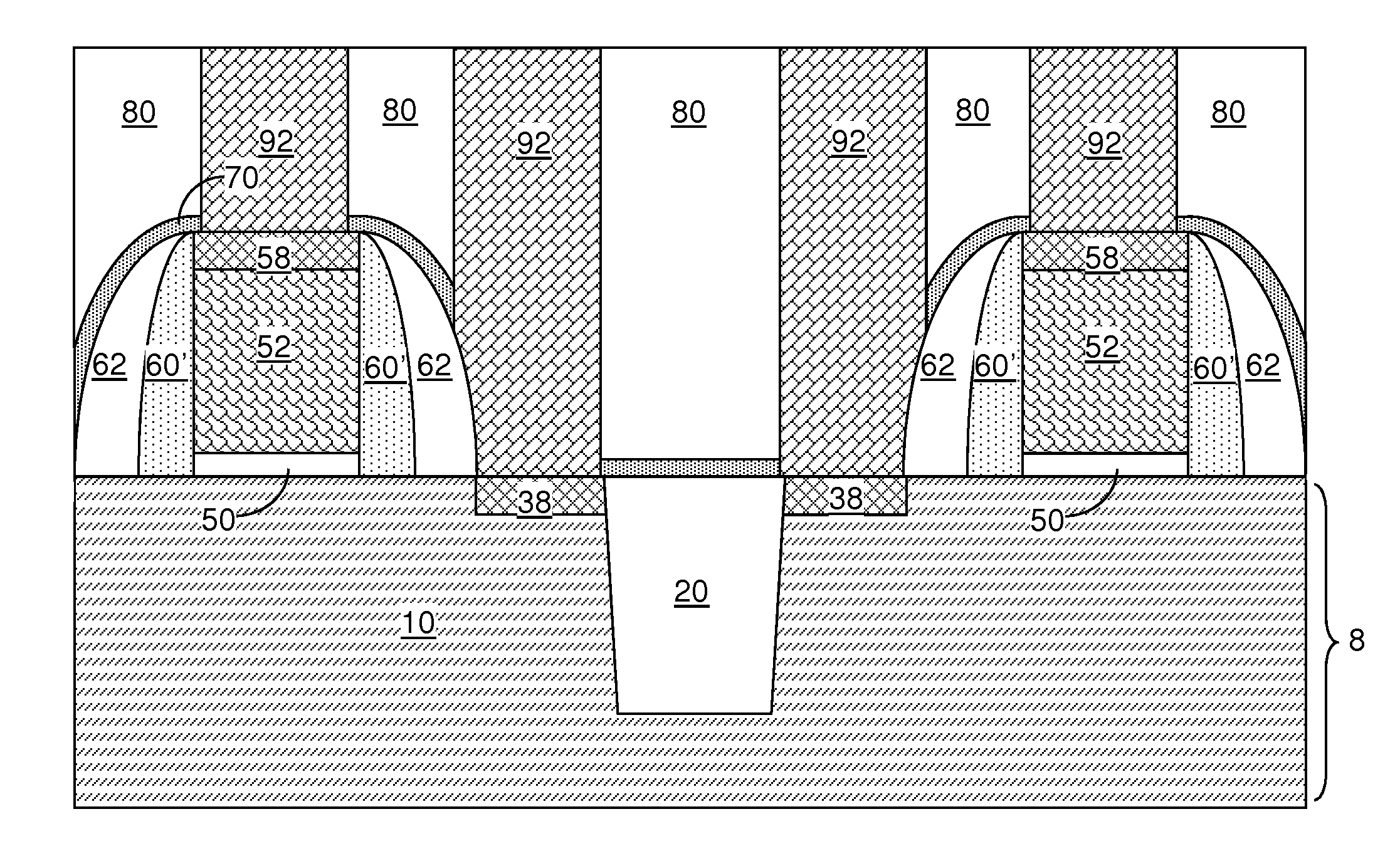
[0054]Referring to FIG. 3, a second exemplary structure according to the present disclosure includes a semiconductor substrate 8, gate stacks formed thereupon, and a silicon nitride layer 60L formed over the semiconductor substrate 8 and the gate stacks. The semiconductor substrate 8 includes a semiconductor layer 10 that includes a semiconductor material portion 10. The semiconductor material portion 10 includes a silicon-based material that can be any of the material that may be employed for the silicon portion 110 described above.

[0055]A shallow trench isolation structure 20 including silicon oxide is formed within the semiconductor material portion 10 in the semiconductor substrate 8. The shallow trench isolation structure 20 can be formed, for example, by forming shallow trenches in the semiconductor material portion 10 and filling the shallow trenches with silicon oxide, which can be deposited, for example, by chemical vapor deposition (CVD). Excess portions of silicon oxide c...


PUM


Abstract

An anisotropic silicon nitride etch provides selectivity to silicon and silicon oxide by forming a fluorohydrocarbon-containing polymer on silicon surfaces and silicon oxide surfaces. Selective fluorohydrocarbon deposition is employed to provide selectivity to non-nitride surfaces. The fluorohydrocarbon-containing polymer interacts with silicon nitride to form a volatile compound, thereby enabling etching of silicon nitride. The fluorohydrocarbon-containing polymer interacts with silicon oxide at a low reaction rate, retarding, or completely stopping, the etching of silicon oxide. The fluorohydrocarbon-containing polymer does not interact with silicon, and protects silicon from the plasma. The anisotropic silicon nitride etch can be employed to etch silicon nitride selective to silicon and silicon oxide in any dimension, including small dimensions less than 50 nm.

Description

BACKGROUND[0001]The present disclosure relates to semiconductor processing methods, and particularly to methods for anisotropically etching silicon nitride with high selectivity to silicon and silicon oxide, and structures for effecting the same.[0002]Etching silicon nitride selective to more than one material is very challenging. Poor performance in selective etching of silicon nitride is often observed especially at the nanoscale level.[0003]An example of poor performance in selectivity of a nitride etch process is observed in the spacer module in which silicon nitride spacers are formed to electrically isolate gate electrodes from source and drain regions. Lack of sufficient selectivity causes formation of recesses within semiconductor material portions that are not covered by the gate electrodes.[0004]Another example of poor performance in selectivity of a nitride etch is observed in a trench silicide etch in which a silicon nitride layer is employed as an etch stop layer. Lack ...

Claims


Application Information

Patent Timeline
IPC IPC(8): H01L29/78H01L21/28H01L21/762
CPCH01L21/31116H01L29/6653H01L21/76802H01L29/6659H01L21/76897H01L29/6656H01L21/31
Inventor CHANG, JOSEPHINE B.ENGELMANN, SEBASTIAN U.FULLER, NICHOLAS C. M.GUILLORN, MICHAEL A.NAKAMURA, MASAHIRO
Owner ZEON CORP
Why Eureka
Try Eureka