Semiconductor device package adapter

a technology of semiconductor devices and package adapters, which is applied in the direction of coupling device connections, printed circuit aspects, printed circuit manufacturing, etc., can solve the problems of pin degradation of signal performance of pga devices, ic devices cannot be connected to the final pcb, and the size and distance between die terminals is so small, so as to increase the overall potential market

Active Publication Date: 2013-05-02
HSIO TECH
View PDF10 Cites 76 Cited by
  • Summary
  • Abstract
  • Description
  • Claims
  • Application Information

AI Technical Summary

Benefits of technology

[0025]Historically, these BGA devices could not be socketed in the final system due to the fact that when contacts engage with the solder ball, the solder creeps away from the ball over time and the connection deteriorates over time. With the present adapter scheme, defective BGA devices can be removed from the PCB. Test facilities can use the mating half of the adapter to run at speed functional test and eliminate the need for test sockets and expensive load boards. The same type of construction can be used for Mezzanine and Backplane connectors, dramatically increasing the overall potential market.
[0026]Test circuitry and software can be embedded into the present adapter to provide intelligent function and the fine feature capability of the process may enable the silicon dies themselves to be attached directly to the adapter eliminating the BGA package altogether and creating a “Pluggable Package”.

Problems solved by technology

In many cases, the size and distance between die terminals is so small that the IC device cannot be connected to the final PCB without some sort of re-routing interface.
The pin on PGA devices degrade signal performance.
The pins are also expensive and are subject to damage during handling.
In relative terms, however, the size of the contacts used in the connectors is very large compared to those used in the LGA type CPU sockets.
These clamping mechanisms apply a fairly significant load to the system, and can cause circuit board warpage, broken solder joints, or flexing of the package.
Next generation LGA devices create many challenges due to the increased performance requirements, multi-core processors which drive the terminal count up, and low voltage differential signal architectures which can challenge terminal routing density.
The challenge is that it is very difficult to make a socket with contacts on a finer pitch that have enough compliance to accommodate the warpage of the package and provide stable contact resistance.
It is also very difficult to route the pattern at the fine pitch and keep the PCB at four layers, unless a very expensive blind and buried via method is used.

Method used


Image

  • Semiconductor device package adapter
  • Semiconductor device package adapter
  • Semiconductor device package adapter

Examples


Embodiment Construction

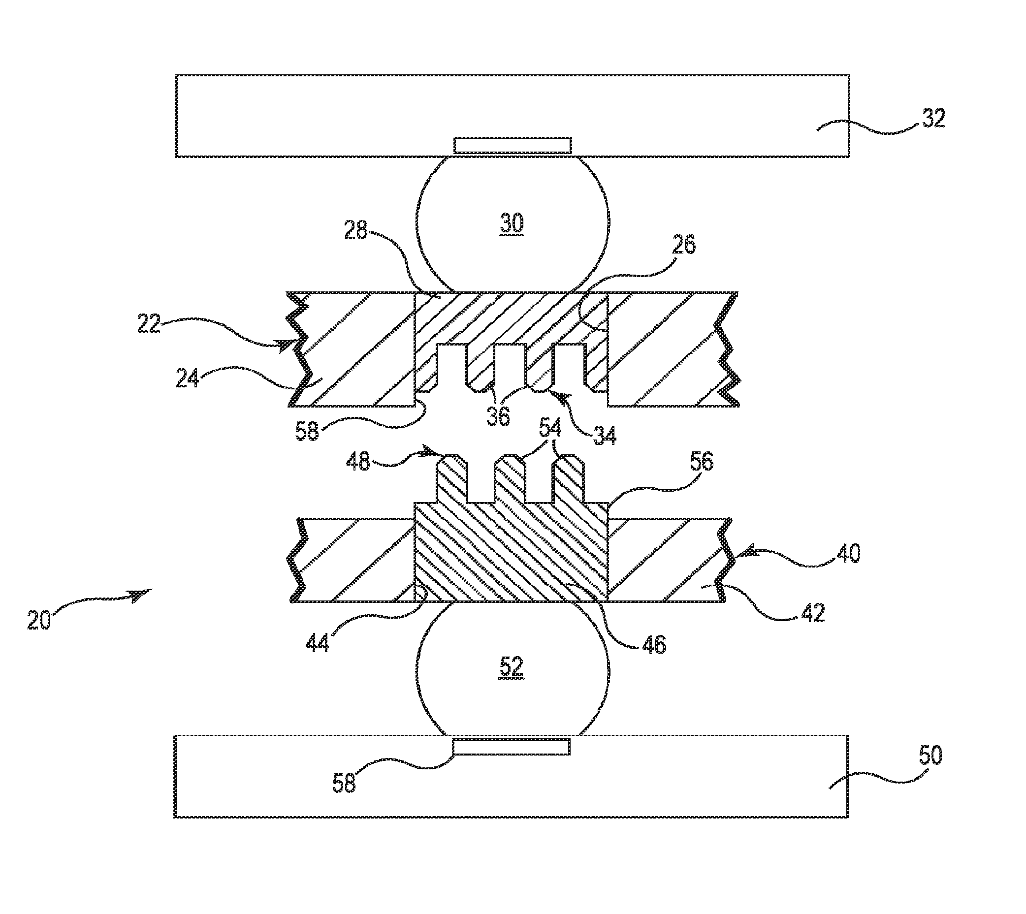
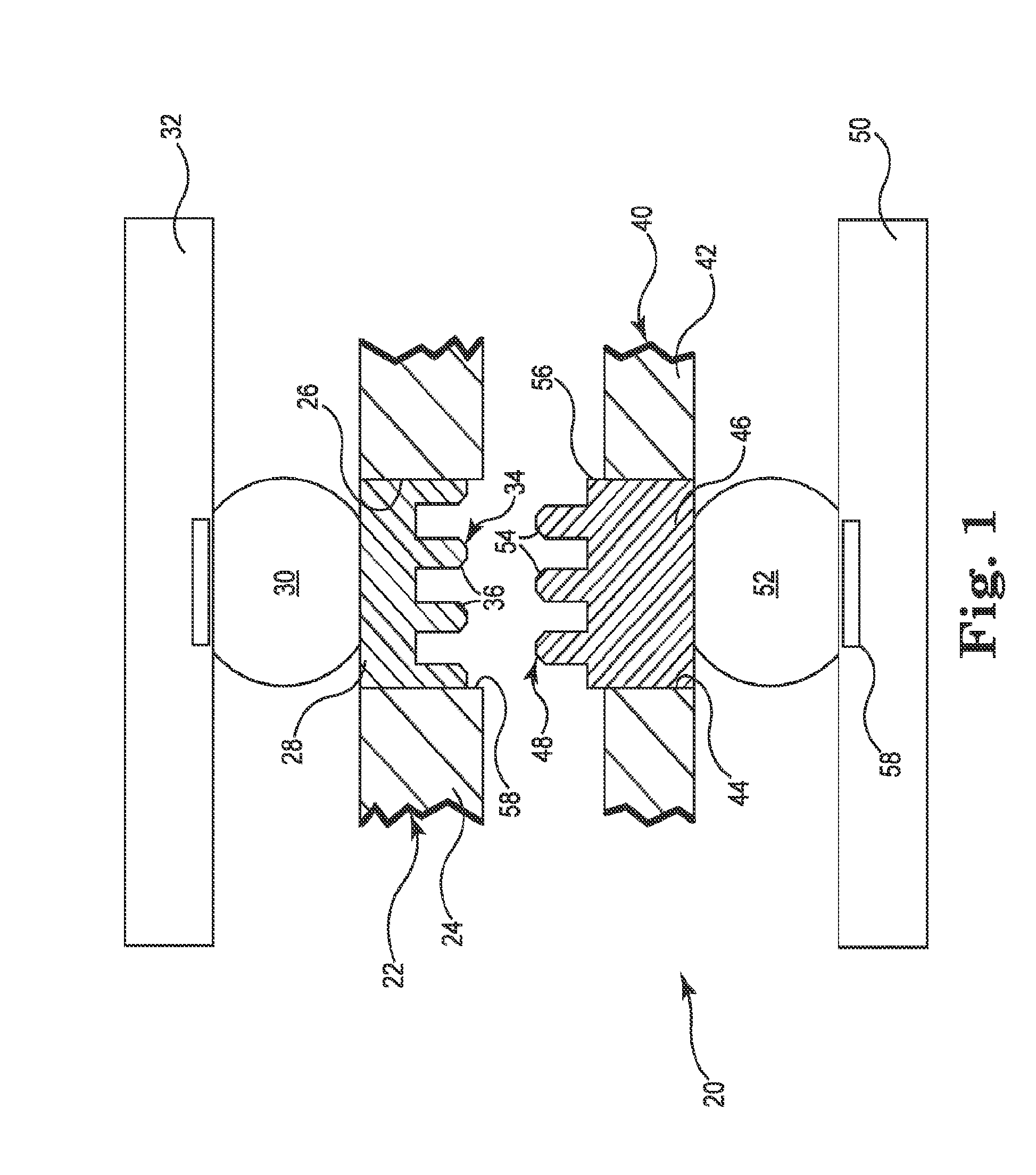
[0055]The present disclosure is directed to an adapter for BGA and LGA packages that can be plugged into a system PCB in a low cost, yet high performance manner, as an alternative to direct solder attachment or PGA substrates. The present adapter permits high performance in the range of about 5-8 GHz signal environment with targeted impedance of 50 ohm single ended.

[0056]FIG. 1 illustrates a semiconductor device package adapter 20 in accordance with one embodiment of the present disclosure. First portion 22 of adapter 20 includes substrate 24 fabricated with simple through-holes 26, that are populated with metallic terminals 28 arranged to correspond with solder balls 30 on BGA device 32. The BGA device 32 is soldered to terminals 28 embedded in the first portion 22 of the adapter 20.

[0057]Second portion 40 also includes substrate 42 with through holes 44, populated with metallic terminals 46 arranged to correspond with contact pads 58 on another circuit member 50, such as a PCB. Th...


PUM


Abstract

A semiconductor device packaged adapter for electrically coupling contacts on a first circuit member to contacts on a second circuit member. The adapter typically includes first and second substrates, each with arrays of terminals. Proximal ends of the first terminals on the first substrate are arranged to be soldered to the contacts on the first circuit member and proximal ends of the) second terminals on the second substrate are arranged to be soldered to the contacts on the second circuit member. Complementary engaging structures located on distal ends of the first and second terminals engage to electrically and mechanically couple the first circuit member to the second circuit member.

Description

TECHNICAL FIELD[0001]The present application is directed to a high performance electrical interconnect between integrated circuits and the intended system circuit board in a removable manner through the use of a packaging adapter.BACKGROUND OF THE INVENTION[0002]Traditional semiconductors and IC devices are typically packaged in a variety of ways to provide redistribution from the terminals on the die to a spacing that is conducive to cost effective printed circuit board (“PCB”) fabrication techniques. The packages also serve to protect the fragile silicon or provide additional functions such as thermal management or near device decoupling. In many cases, the size and distance between die terminals is so small that the IC device cannot be connected to the final PCB without some sort of re-routing interface.[0003]Historically, pin grid array packages (“PGA”) were used for CPU devices. A socket was soldered to the motherboard and the field of pins extending out of the package was plug...

Claims


Application Information

Patent Timeline
Patent Type & Authority Applications(United States)
IPC IPC(8): H01L23/00
CPCH01R12/7076H01R13/6474H01L2924/1306H01L2924/10253H01L2924/01029H01R13/6585H01R2201/20H01L24/14H01L24/81H01L23/552H01L24/19H01L24/20H01L25/0655H01L25/0657H05K3/32H05K3/3436H01L2224/04105H05K2201/10378H05K2201/1059H05K2201/10734H05K2201/10962H01L2924/00H01L2924/12042H01L2224/0401H01L2924/14
Inventor RATHBURN, JAMES
Owner HSIO TECH
Why Eureka
Try Eureka