
Photoelectric conversion cell and array, reading method therefor, and circuit thereof

a conversion cell and array technology, applied in the direction of radio frequency control devices, instruments, television systems, etc., can solve the problems of limiting the accuracy of information detection, limiting the free range of mutual pixel interference and information detection at low illumination, and the collector is difficult to be sufficiently thick in a direction, so as to prevent the miller effect, increase the reading delay, and easy to separate the signal from the noise

Inactive Publication Date: 2013-05-16
NAT INST OF ADVANCED IND SCI & TECH
View PDF1 Cites 6 Cited by
  • Summary
  • Abstract
  • Description
  • Claims
  • Application Information

AI Technical Summary

Benefits of technology

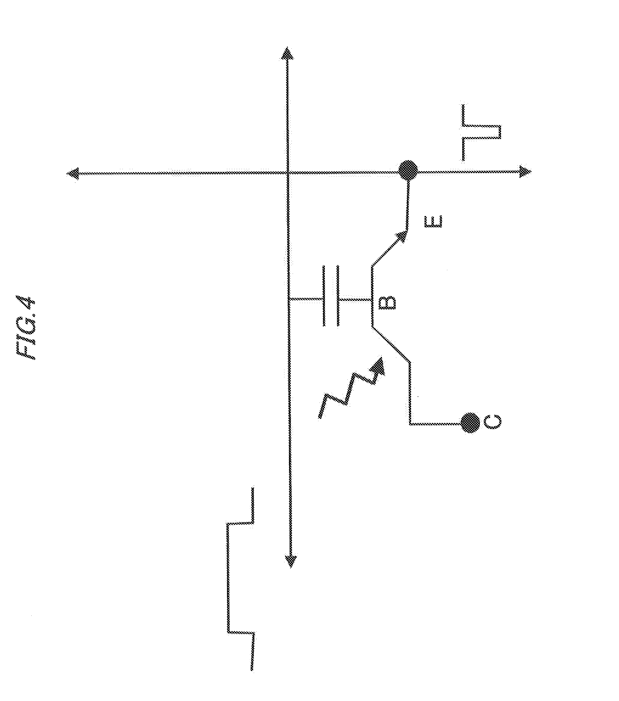
[0165]According to the present invention, if the photoelectric conversion element is a phototransistor and a signal is obtained not from the collector but from the emitter a reading delay caused by stray capacitance between the collector and each of the isolation region and the substrate is avoided, and an increase of the reading delay because of the Miller effect is prevented. In the case of the photoelectric conversion cell C1, current amplification is also performed when the address selection is performed by the emitter. According to the present invention, image information can be read at sensitivity close to dark current limitation.
[0166]The connection method of the selection element and the photoelectric conversion element can control disturbances including a voltage variation given in a reading pixel or in another pixel in response to a noise and a voltage variation on the signal output line during reading.
[0167]Since the connection method of the first transistor of the present invention makes a feed-through noise of an address selection pulse (a pulse applied to the first selection line, the second selection line, or the third output line) at a leading pulse edge to be opposite in sign to the read signal, it is easy to separate the signal from the noise. The effect of the noise can be eliminated by slicing the read signal through a strobe process or the like after the leading-pulse-edge ...

Problems solved by technology

A time delay in reading is further caused by stray capacitances between the collector and each of a substrate and an isolation region.
For this reason, there has been a limitation to precision detection free from mutual pixel interference and information detection at low illuminance level.
The structure that needs the collector to be isolated from the substrate in this way is hard to make the collector to be sufficiently thick in a direction of the depth of the collector.
Then, it is very difficult to realize high sensitivity down to a wavelength corresponding to near the band gap energy of the semiconductor forming collector by using the semiconductor, such as silicon, having a small light-absorption coefficient in the infrared region.
If the collector of another phototransistor is connected to the collector, a floating potential interacts with a storage state of optical information of the other phototransistor, causing a disturbance.
If the array originally not intended for a two-dimensional array is attempted to be two-dimensional arrayed by merely connecting a plurality of collectors in a two-dimensional arrangement, a two-dimensional array with small mutual interference in pixel information is difficult to realize.
If an emitter of another phototransistor is connected to the emitter in an attempt to design a two-dimensional array, the floating potential interacts with a storage state of optical information of the other phototransistor, causing a disturbance.
If a plurality of the emitters in the one-dimensional array merely connected, a two-dimensional array with small mutual interference in pixel information is difficult to realize.
Even if a two-dimensional array is designed in accordance with the technique disclosed in Patent Document 1, there is a limitation to precision detection free from mutual pixel interference and to pixel information detection at low illuminance level.
If a peripheral circuit such as a address selection circuit is implemented using MOSLSI, the technique is not advantageous in terms of quality and number of the manufacturing processes.
However, this technique also causes a disturbance to all deselected pixels having the electric capacitance connected to the one address selection line.
There is still a limitation on the detection of an image signal at low illuminance level.
If a two-dimensional array is assembled in accordance with the related art technique, the address selection noise gives a limitation on the detection of a low-illuminance level image signal.
This not only restricts the operation of a circuit connected to the signal output line, but also causes the noise on the signal output line to enter into the pixel.
Since the disclosed phototransistor one-dimensional array does not have a pixel architecture that is intended to be applied into a two-dimensional array, the phototransistor one-dimensional array is not appropriate as a candidate for a pixel architecture for the two-dimensional array.

Method used


Image

  • Photoelectric conversion cell and array, reading method therefor, and circuit thereof
  • Photoelectric conversion cell and array, reading method therefor, and circuit thereof
  • Photoelectric conversion cell and array, reading method therefor, and circuit thereof

Examples


embodiments

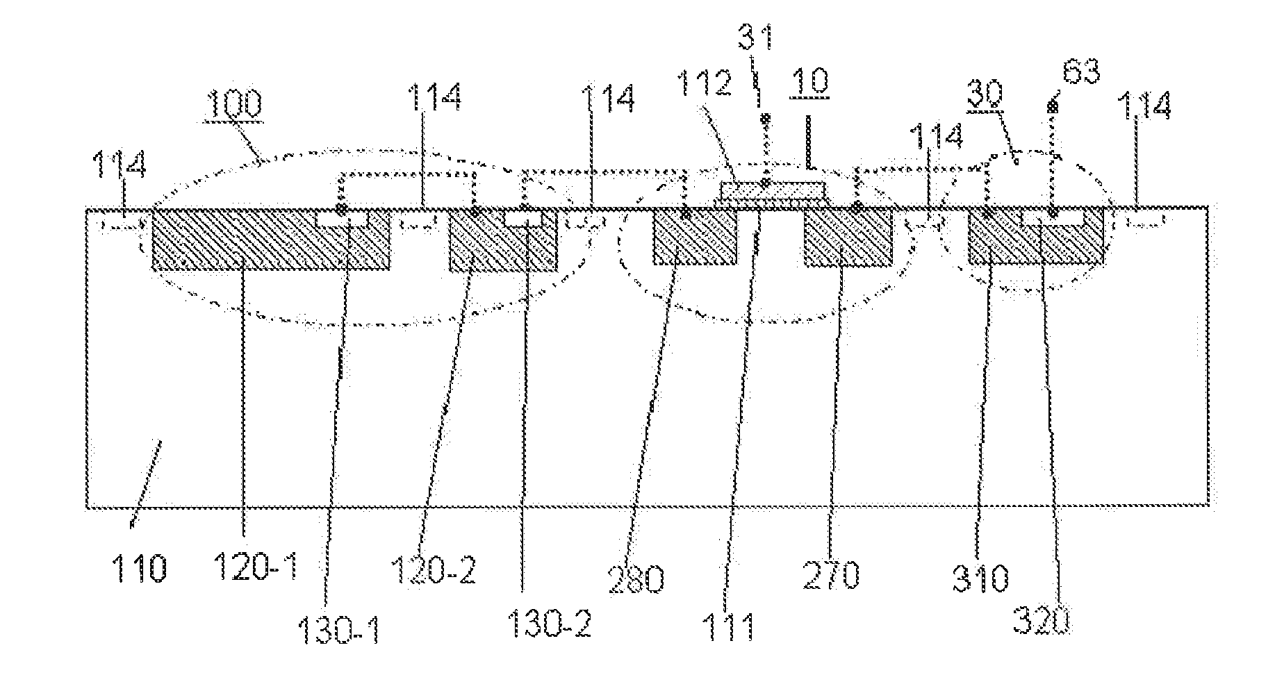
[0329]A structure example A1str of the photoelectrical conversion cell A1 of the present invention is described below. More specifically, the photoelectric conversion cell A1str includes, at least, a first semiconductor region having a first surface and a first conductivity type, one or plural second semiconductor regions, each having a second surface, and a conductivity type opposite to the first conductivity type, and provided on or in the first surface of the first semiconductor region, one or plural third semiconductor regions, each having a third surface and the first conductivity type, each third semiconductor region provided on and / or in the second surface of the second semiconductor region, a seventh semiconductor region having a seventh surface and the conductivity type opposite to the first conductivity type, and spaced apart from the second semiconductor region, on or in the first surface of the first semiconductor region, an eighth semiconductor region having an eighth s...


PUM


Abstract

In order to achieve a photovoltaic cell and an array of high sensitivity and high dynamic range, there is a need for a photovoltaic cell and an array which are combined so that an amplified photovoltaic element and a selection element are resistant to external noise, and so that the combination is resistant to effects from address selection pulse noise at array readout time. In the present invention, in order to solve the problem, a photovoltaic cell has been configured with a combination of an amplified photovoltaic element (100) and a selection element (10 and the like) which are resistant to external noise, and various means of solution of the combination are provided which are resistant to the effects of address selection pulse noise at array readout time. As a result, a dynamic range of 6 to 7 orders of magnitude for light detection has become possible.

Description

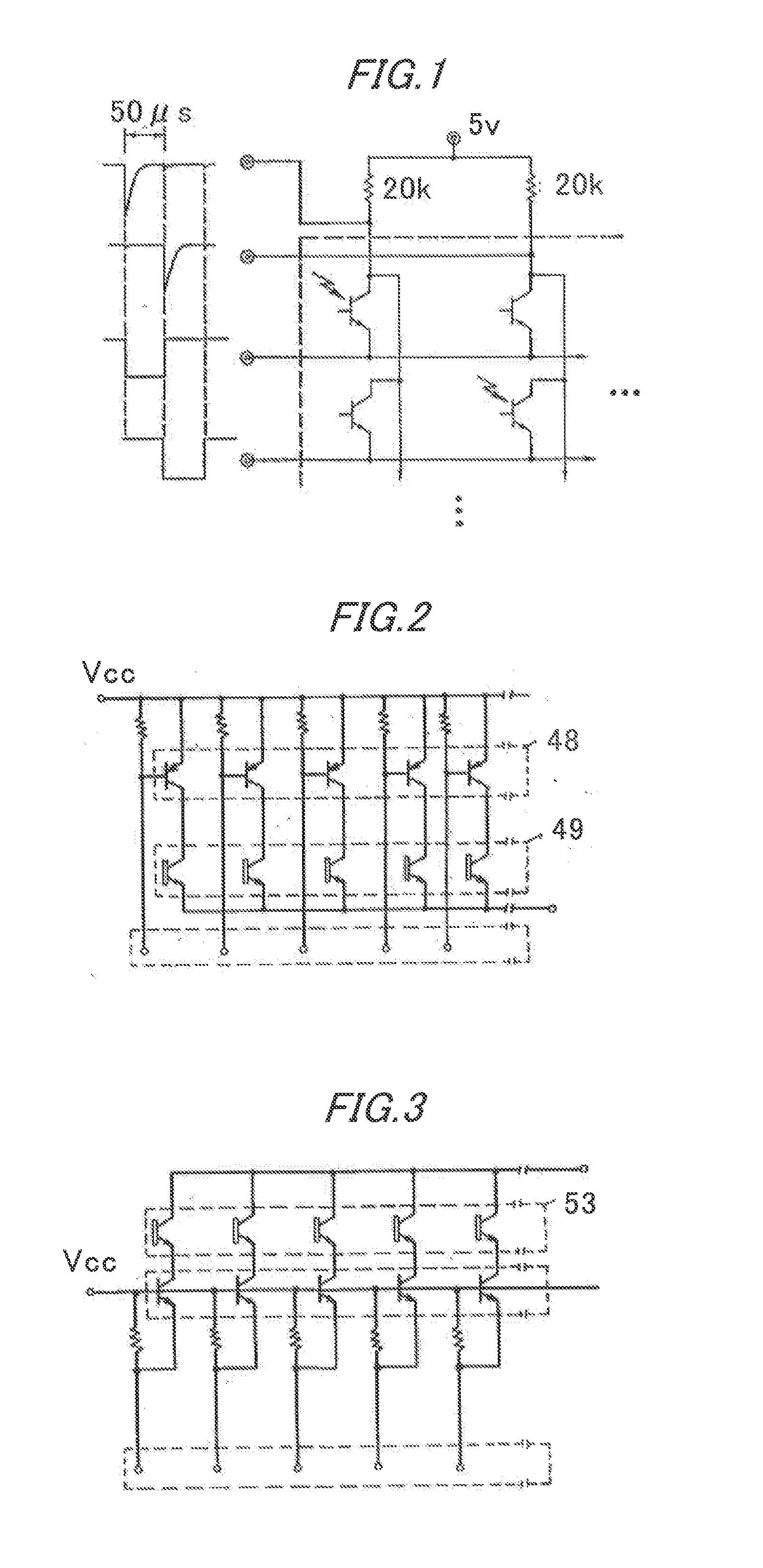
TECHNICAL FIELD[0001]The present invention relates to a photoelectric conversion cell that converts light into an electrical signal, and an array that employs the cells. The present invention also relates to a reading method of the cells and array.BACKGROUND ART[0002]In order to read image information from a two-dimensional array of conventional phototransistors, each phototransistor serving as a pixel has an emitter connected to a word line, and a collector connected to a bit line and to a load resistor as illustrated in FIG. 1, and the image information is read from the collector (FIG. 1 is quoted from FIG. 5 in Patent Document 1). A time delay in reading calculated from collector-base capacitance and a load resistance is increased due to the Miller effect, in which a collector potential changes in response to an output signal. A time delay in reading is further caused by stray capacitances between the collector and each of a substrate and an isolation region. A dark current of th...

Claims


Application Information

Patent Timeline
IPC IPC(8): H01L27/146H01L31/101
CPCH01L27/1446H01L31/103H01L31/101H01L27/14609H04N5/361H04N25/63
Inventor HAYASHI, YUTAKANAGAMUNE, YASUSHIOTA, TOSHITAKA
Owner NAT INST OF ADVANCED IND SCI & TECH
Learn More