

Silicon carbide semiconductor device and method for manufacturing the same
a technology of silicon carbide and semiconductor devices, which is applied in the direction of semiconductor devices, basic electric elements, electrical appliances, etc., can solve the problem of difficulty in and achieve the effect of convenient filling the gate electrode into the trench and preferable channel characteristics
- Summary
- Abstract
- Description
- Claims
- Application Information
AI Technical Summary
Benefits of technology
Problems solved by technology
Method used
Image

Examples
embodiment 1
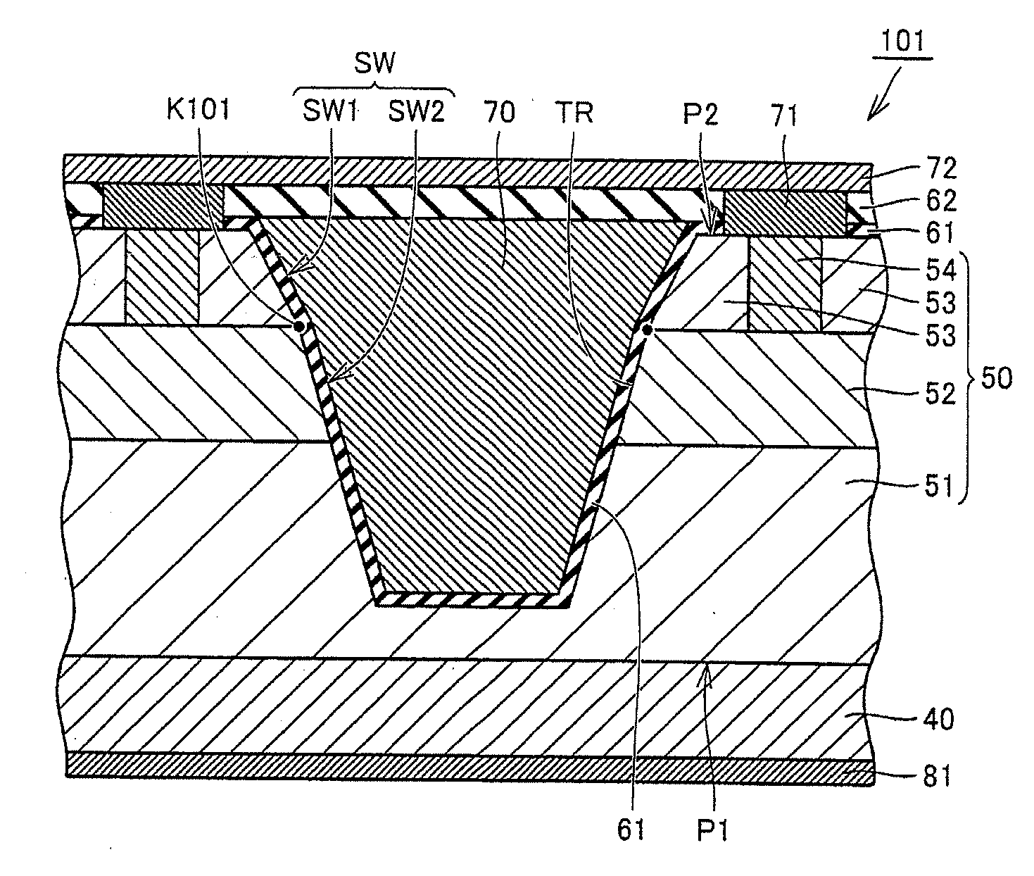
[0046]As shown in FIG. 1, a MOSFET (Metal Oxide Semiconductor Field Effect Transistor) 101 as a silicon carbide semiconductor device in accordance with the present embodiment has a substrate 40, an epitaxial layer (silicon carbide layer) 50, a gate insulating film 61, an interlayer insulating film 62, a gate electrode 70, a source electrode 71, a source wire electrode 72, and a drain electrode 81.
[0047]Substrate 40 is made of an n type (first conductivity type) semiconductor or conductor, and is preferably a single crystal silicon carbide substrate. Drain electrode 81 is provided on one side of substrate 40, and epitaxial layer 50 is provided on the other side of substrate 40. Drain electrode 81 is an ohmic electrode.
[0048]Epitaxial layer 50 has a thickness direction (vertical direction in the drawing), and has a lower surface (first main surface) P1 facing substrate 40 and an upper surface (second main surface) P2 opposite to lower surface P1 in the thickness direction. When epitax...
embodiment 2
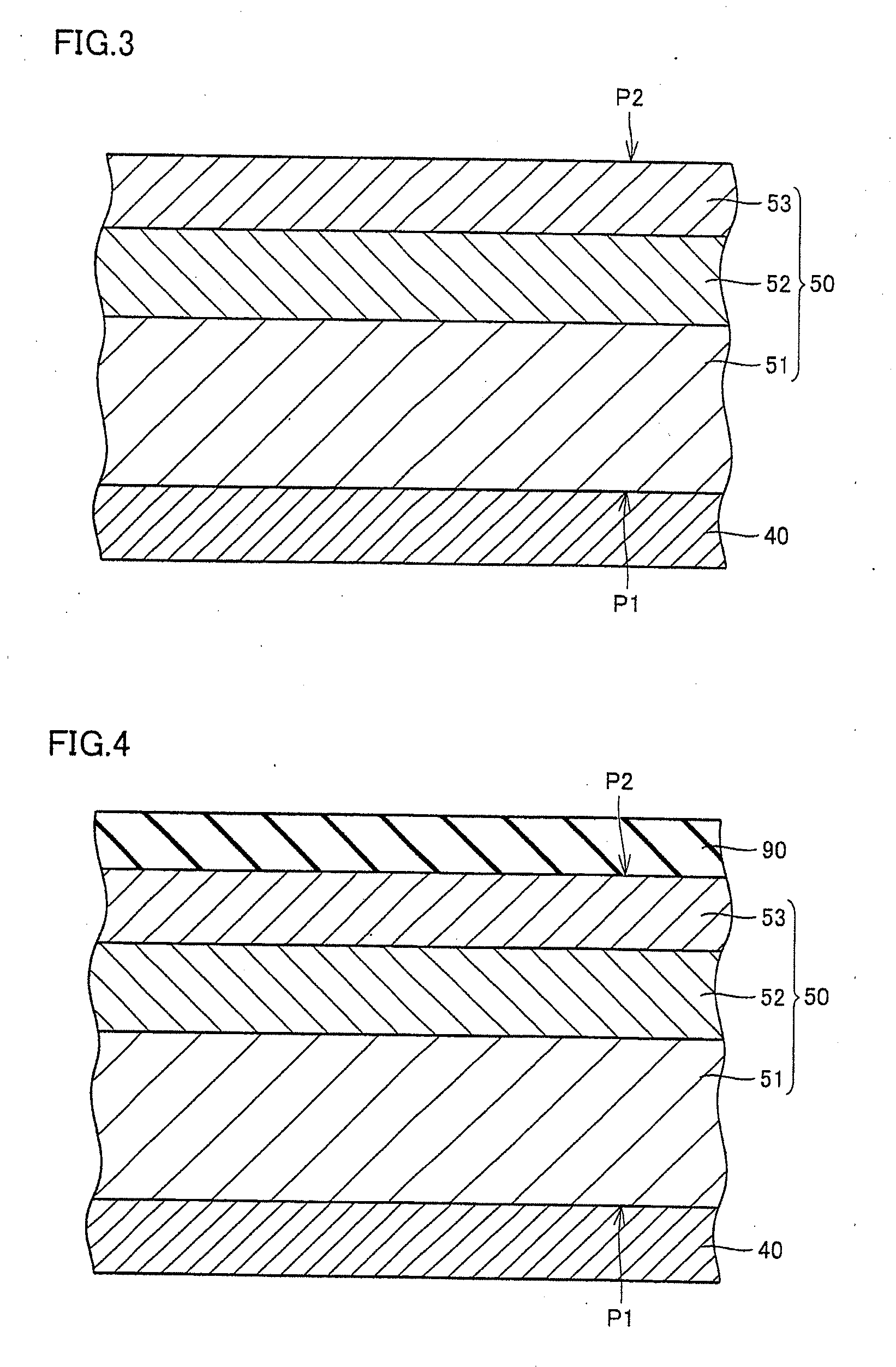
[0072]In the present embodiment, firstly, the steps identical to those in up to FIG. 5 in Embodiment 1 are performed. Next, as shown in FIG. 11, an altered layer 99 is formed in epitaxial layer 50 by implanting ions into epitaxial layer 50 using mask 90. Preferably, the step of forming altered layer 99 is performed such that altered layer 99 is located shallower than second region 52. Preferably, the step of forming altered layer 99 is performed at normal temperature. Subsequently, thermal etching identical to that in Embodiment 1 is performed. In this case, in the first half of the thermal etching, a region of epitaxial layer 50 including altered layer 99 is removed as shown in FIG. 12. A concave portion thereby formed has a bending point K2. Since the steps other than that are substantially identical to those in Embodiment 1, the description thereof will not be repeated.
[0073]According to the present embodiment, altered layer 99 is formed in epitaxial layer 50 by implanting ions i...
embodiment 3
[0076]In the present embodiment, in the ion implantation for forming third region 53 (FIG. 3) in Embodiment 1, a method which is particularly likely to cause crystal defects is selected. For example, the ion implantation for forming third region 53 is performed at normal temperature. As a result, crystallinity of third region 53 is sufficiently lower than crystallinity of second region 52. Thereafter, the steps identical to those in up to FIG. 5 in Embodiment 1 are performed. Next, thermal etching identical to that in Embodiment 1 is performed. In this case, in the first half of the thermal etching, third region 53 of epitaxial layer 50 is removed as shown in FIG. 13. A concave portion thereby formed has a bending point K3. Then, through the second half of the thermal etching, trench TR is formed, for example, as shown in FIG. 14. Since the steps other than that are substantially identical to those in Embodiment 1, the description thereof will not be repeated.
[0077]According to the ...
PUM
 Abstract
Description
Claims
Application Information