

High density six transistor finfet SRAM cell layout
a technology of sram cell and high density, applied in the direction of transistors, semiconductor devices, electrical equipment, etc., can solve the problems of limiting the amount of other logic that can be provided, imposing a longer access time, etc., and achieve convenient and reliable connection formation, high scalable effect, and improved fin formation fidelity
- Summary
- Abstract
- Description
- Claims
- Application Information
AI Technical Summary
Benefits of technology
Problems solved by technology
Method used
Image

Examples
Embodiment Construction
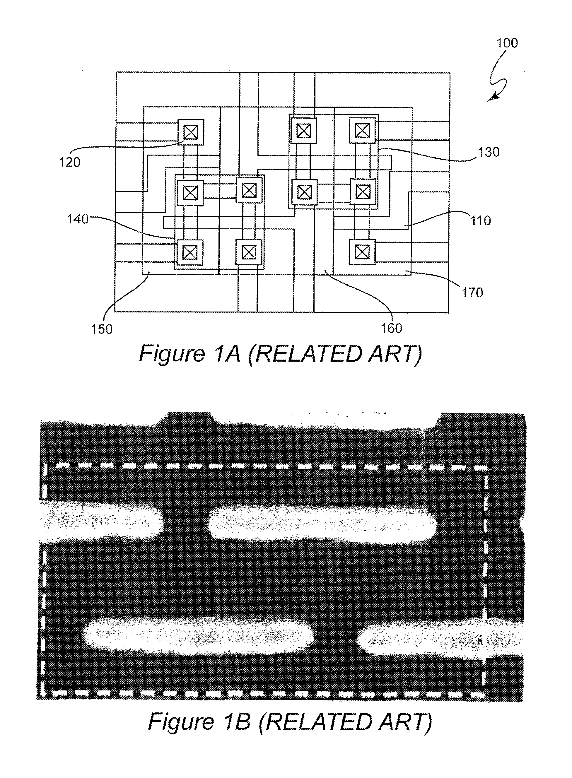
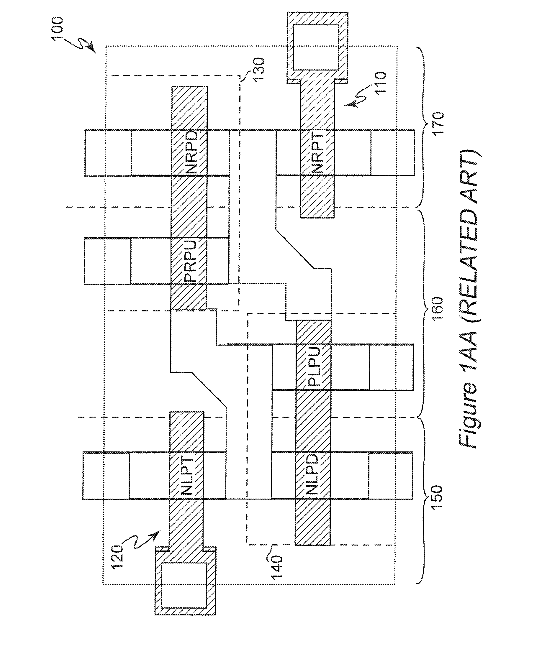
[0020]Referring now to the drawings, and more particularly to FIG. 1A, there is shown a plan view of the layout of a known SRAM cell including six transistors and sufficient to store a single bit (thus, sometimes referred to hereinafter as a bit-cell). FIG. 1AA is an enlarged schematic depiction of the plan view of the bit-cell layout of FIG. 1A. The transistors are indicated with the same reference numerals in both FIGS. 1A and 1AA. FIG. 1B is a scanning electron microscope (SEM) image of a device having the same layout but prior to the application of connections shown in FIG. 1A. The brighter, horizontal areas appearing in FIG. 1B are polysilicon gates while the darker, vertical areas of FIG. 1B are the FinFET fins.
[0021]As a compromise between performance and complexity, an SRAM memory cell usually comprises six transistors although as few as four transistors or eight or more transistors can be used in each SRAM cell. Using only four transistors requires inclusion of resistors wh...
PUM
 Abstract
Description
Claims
Application Information