Field emission light source device and manufacturing method thereof

a field emission and light source technology, applied in the field of vacuum electron devices, can solve the problems of shortening the life of field emission devices and reducing the vacuum degree of field emission light source devices, and achieve the effects of stable electron-impact resistance performance, good electrical conductivity, and high light transmittan

Active Publication Date: 2013-07-04
OCEANS KING LIGHTING SCI&TECH CO LTD
View PDF6 Cites 0 Cited by
  • Summary
  • Abstract
  • Description
  • Claims
  • Application Information

AI Technical Summary

Benefits of technology

[0022]By using transparent ceramic as the base of the anode plate and taking its advantages of good electrical conductivity, high light transmittance, stable electron-impact resistance performance and uniform luminescence, electron beam excitation efficiency and light extraction efficiency of a field emission light source device can be increased, resulting in improvement of luminous efficiency of a field emission light source device.

Problems solved by technology

However, in the anode plate using sulfides phosphor having good electrical conductivity, decomposition of sulfides may occur easily and emit gas, which not only decreases the vacuum degree of field emission light source device but poisons the cathode, and ultimately shortens the life of a field emission device.

Method used


Image

  • Field emission light source device and manufacturing method thereof
  • Field emission light source device and manufacturing method thereof
  • Field emission light source device and manufacturing method thereof

Examples


example 1

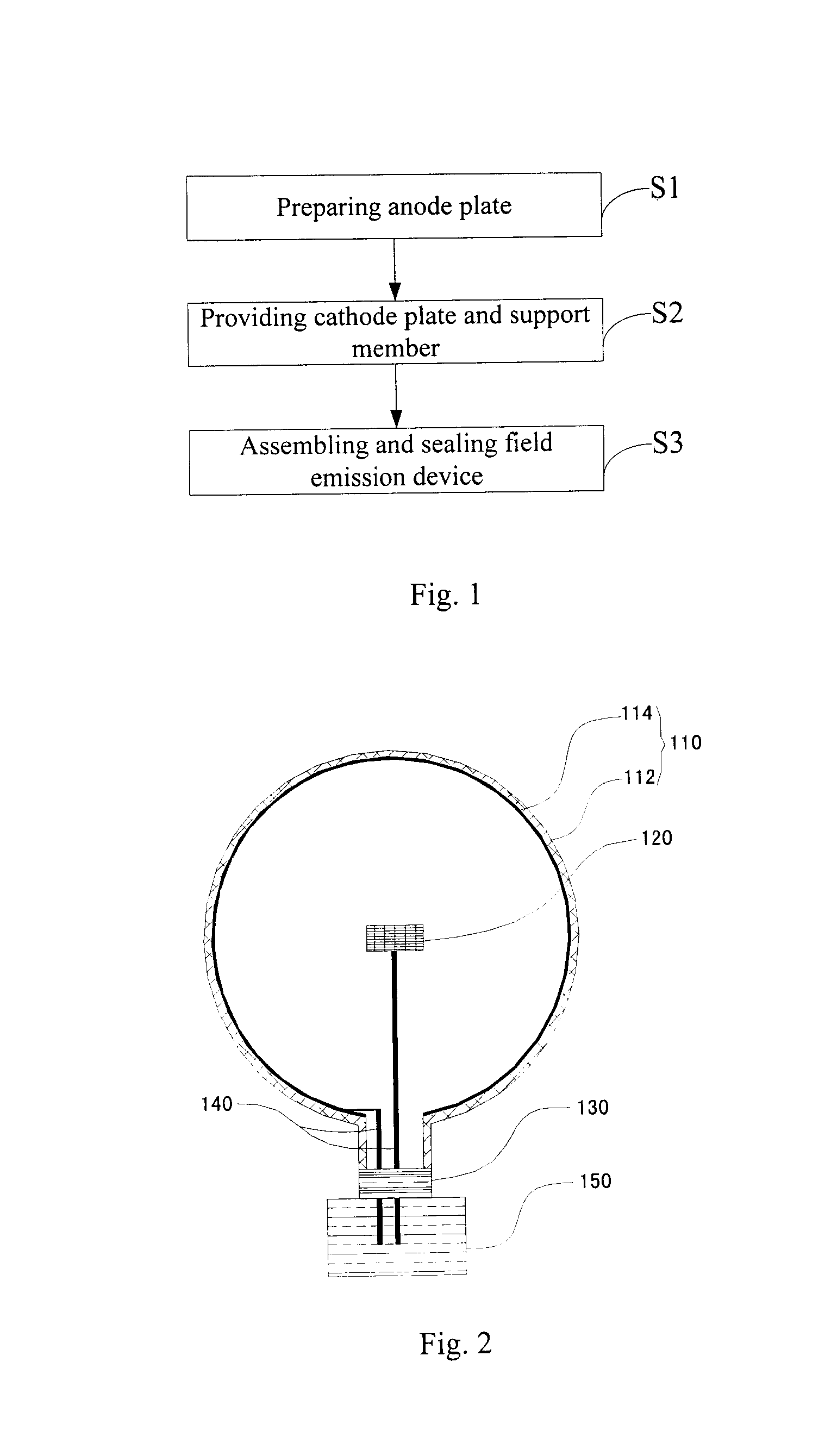
[0049]FIG. 2 shows a structure diagram of field emission light source device of Example 1, comprising a spherical anode plate 110 having a diameter of 100 mm, cathode plate 120 in the size of 70×60×25 mm, insulating support member 130, wires 140 and powder supply 150. The spherical anode plate 110 comprises a base 112 and anode conductive layer 114 disposed on the internal surface of the base 112. Cathode plate 120 is disposed on the centre of the spherical anode plate 110. Cathode plate 120 comprises ITO thin film layer disposed on a surface of the substrate and CNT layer disposed on the ITO thin film layer. Anode plate 110 and cathode plate 120 are spaced apart from each other and fixed by support member 130. Two wires 140 cross the support member 130, whose one end is connected to anode conductive layer 114 and cathode conductive layer 120, the other end is connected to powder supply 150.

[0050]Al2O3 is used as the material of support member 130 for insulating and fixing; in other...

example 2

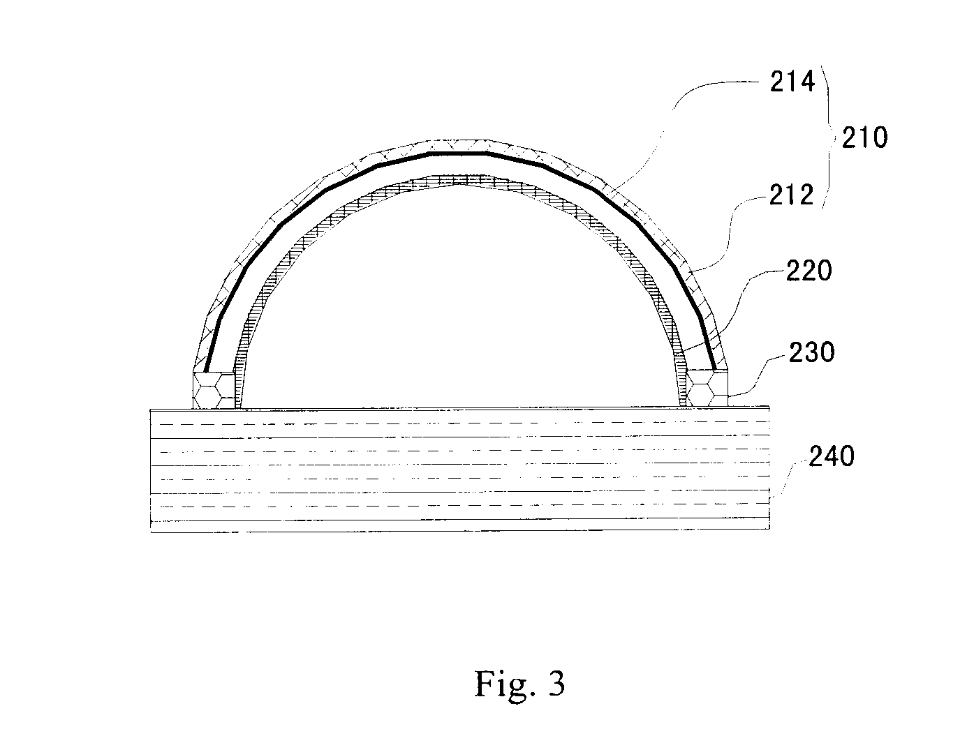
[0060]FIG. 3 shows a structure diagram of field emission light source device of Example 2, comprising a curved anode plate 210 having a chord of 50 mm, cathode plate 220, insulating support member 230 and powder supply 240. The anode plate 210 comprises a base 212 and anode conductive layer 214 disposed on the base. The configuration of cathode plate 220 is generally consistent with the internal surface of anode plate 210, and cathode plate 220 is disposed in parallel with the internal surface of anode plate 210. Cathode plate 220 comprises ITO thin film layer disposed on a surface of the substrate and CNT layer disposed on the ITO thin film layer. Anode plate 210 and cathode plate 220 are spaced apart from each other and fixed on the shell of power supply 240 by support member 230.

[0061]ZrO2 is used as the material of support member 230 for insulating and fixing; in other embodiments, Al2O3 can also be used as the material of support member.

[0062]Material of the base 212 can be Y2S...


PUM

PropertyMeasurementUnit
visible light transmittanceaaaaaaaaaa
thickaaaaaaaaaa
diameteraaaaaaaaaa

Abstract

A field emission light source device, comprising: cathode plate comprising substrate and cathode conductive layer disposed on surface of substrate, and anode plate comprising base formed from transparent ceramic material and anode conductive layer disposed on one surface of base, and insulating support member by which cathode plate and anode plate are integrally fixed, and vacuum-tight chamber formed with anode plate, cathode plate and insulating support member; anode conductive layer and the cathode plate are disposed opposite each other. Because of advantages of good electrical conductivity, high light transmittance, stable electron-impact resistance performance and uniform luminescence, using transparent ceramic as the base of the anode plate in the field emission light source device can increase electron beam excitation efficiency effectively, increase light extraction efficiency of the field emission light source device, and finally increase its luminous efficiency. A manufacturing method of the field emission light source device is also provided.

Description

FIELD OF THE INVENTION[0001]The present invention relates to vacuum electron devices. More specifically, the present invention relates to a field emission light source device and manufacturing method thereof.BACKGROUND OF THE INVENTION[0002]Field emission light source, an emerging light source having features of large current density, low power consumption, fast responding, etc, has important application prospects in the field of flat-panel display, X-ray source, microwave amplifier and other vacuum electronics fields. The working principle of field emission source is: in the electric field, metal tip at low potential, carbon nano tube and other electron emitters emit electrons that strike phosphor at high potential to produce visible light.[0003]Traditional field emission light source device which has advantages of low operating voltage, no warm-up delay, being highly integrated, energy saving, being environmentally friendly, quick start, being thin and light, good environmental su...

Claims


Application Information

Patent Timeline
Patent Type & Authority Applications(United States)
IPC IPC(8): H01J1/90H01J9/38
CPCH01J63/06H01J1/90H01J9/24H01J61/30H01J63/02H01J9/38
Inventor ZHOU, MINGJIEMA, WENBOLI, QINGTAO
Owner OCEANS KING LIGHTING SCI&TECH CO LTD
Why Eureka
Try Eureka